

Solid state radiation detector
- Summary
- Abstract
- Description
- Claims
- Application Information
AI Technical Summary
Problems solved by technology
Method used
Image

Examples
Embodiment Construction
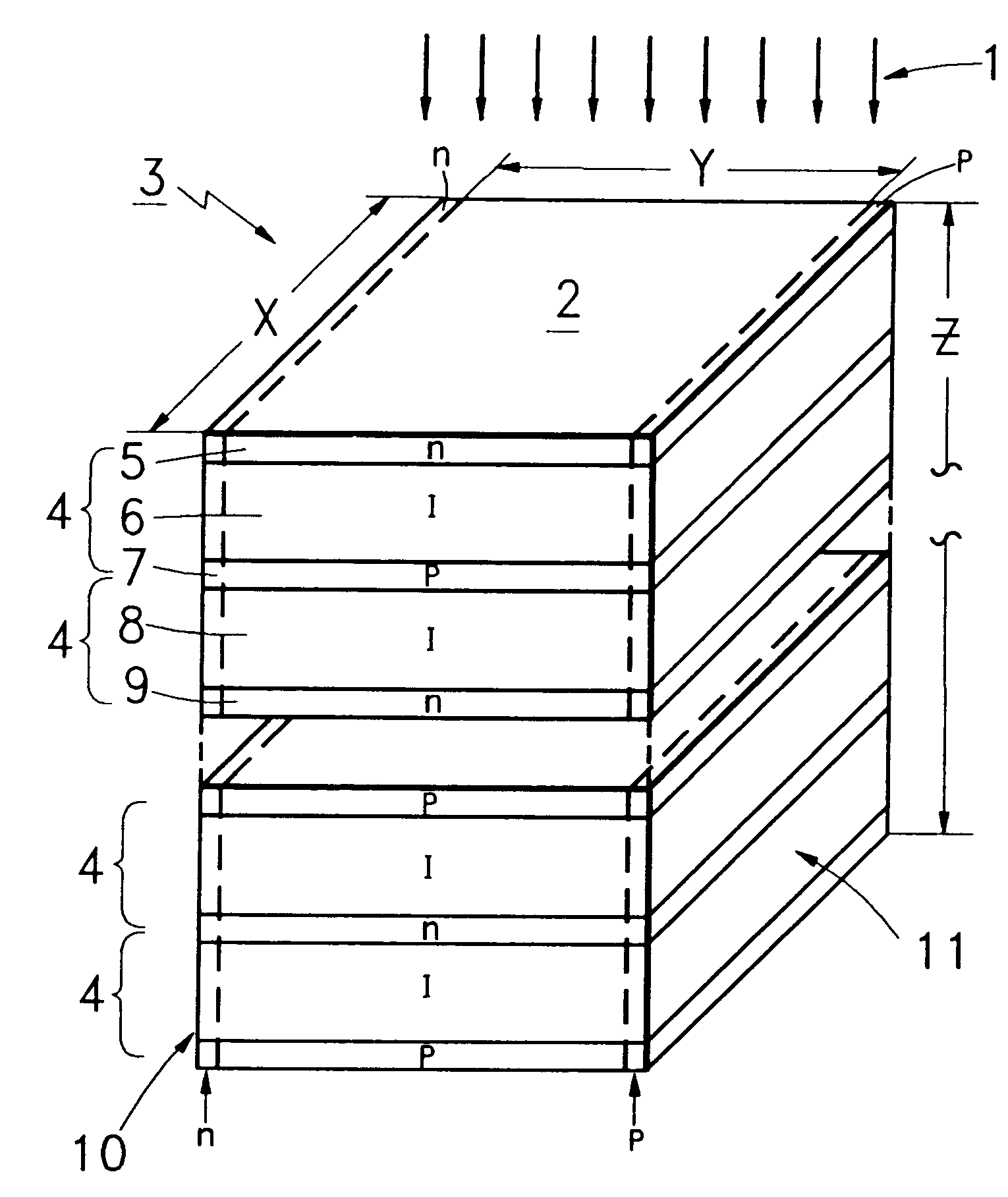
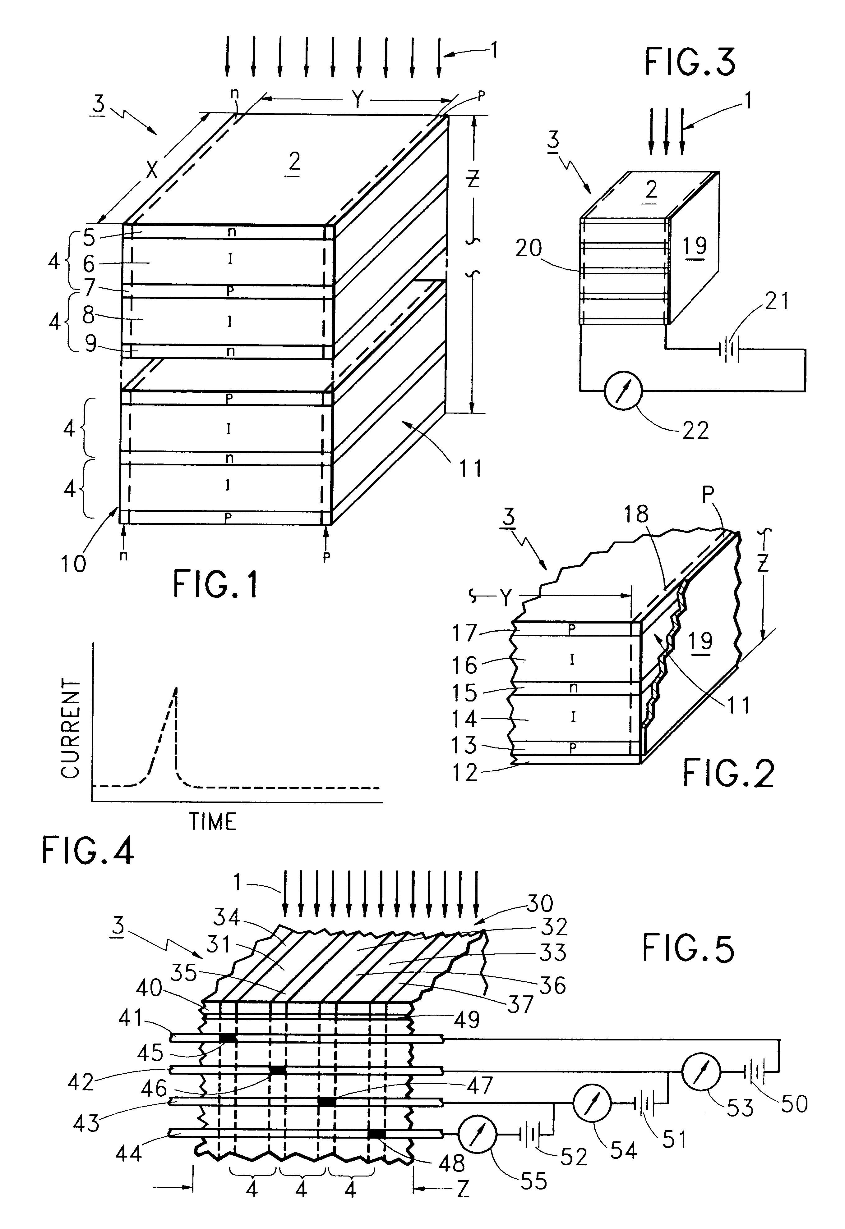
In accordance with the invention, the atomic particles of the radiation are absorbed in a plurality of relatively thick absorbtion members. Each absorbtion layer is made up of a preferably monocrystalline, high density, high band gap, semiconductor material that is depleted of conduction carriers and has a relatively thin conductive layer on each side for external contact.
In one type of construction the relatively thin conductive layers are made up of a layer of one conductivity type on one side of the absorbtion layer and a layer of the opposite conductivity type on the other side of the absorbtion layer.
In another type of construction the thin layers are of a metal. The thin conductive layers, under bias, impress a carrier sweeping field across the depleted absorbtion layer for any carriers that are the result of a collision event by an atomic particle.
In one embodiment, there are as many absorption members, serially positioned as a stack, along the absorbtion path, as are needed ...
PUM
 Abstract
Description
Claims
Application Information