Liquid crystal display device

a display device and liquid crystal technology, applied in the direction of instruments, static indicating devices, etc., can solve the problems of waveform distortion, improper luminance increase or decrease, flicker on the display screen,

Inactive Publication Date: 2001-02-20
KK TOSHIBA
View PDF6 Cites 30 Cited by
  • Summary
  • Abstract
  • Description
  • Claims
  • Application Information

AI Technical Summary

Problems solved by technology

However, actually, since the driver 2 has a certain, non-zero output impedance value, a low-pass filter is formed by a parasitic capacitance in the liquid crystal panel 1 and the output impedance of the driver 2, which causes a problem that waveform distortion occurs as indicated by the continuous line and a flicker occurs on the display screen.
Since pixels for which polarity inversion is effected with respect to the preceding field and pixels for the next signal writing are continuously given signals of the same polarity, waveform distortion of signal voltages due to the output impedance of the signal line driver causes a problem that the luminance increases or decreases improperly or a flicker occurs on the display screen.
This is because if the interval is longer than the above time constant, the absolute value of the signal line driver output in the dummy cycle becomes different from that during actual writing, to cause a flicker in a displayed image.
This is because where a ferroelectric liquid crystal layer or an antiferroelectric liquid crystal layer is used, large depolarization current requires a sufficiently long writing time or a sufficiently large write voltage.

Method used


Image

  • Liquid crystal display device
  • Liquid crystal display device
  • Liquid crystal display device

Examples


first embodiment

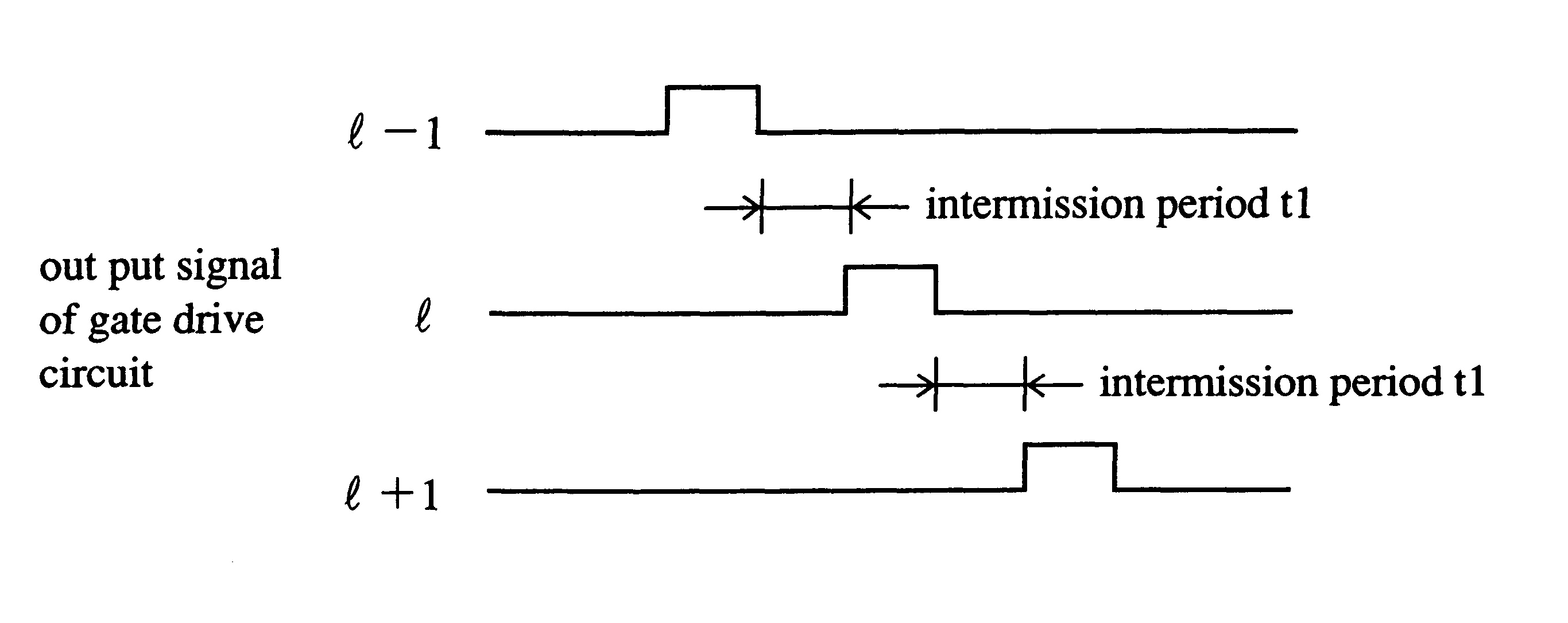
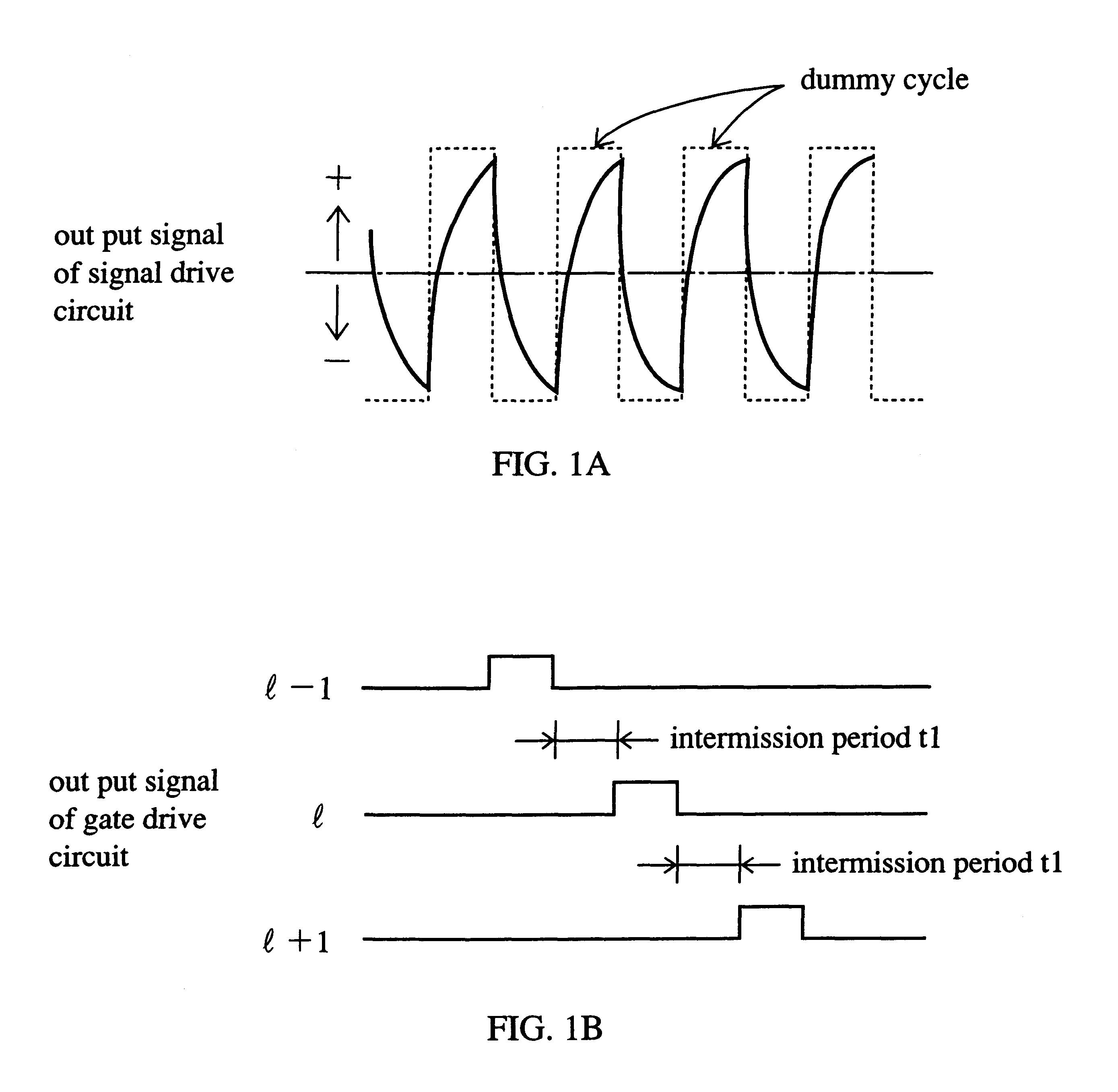
FIG. 1 shows signal waveforms according to the invention. Specifically, FIG. 1A shows an output signal of a signal line driver and FIG. 1B shows output signals of a scanning line driver (i.e., gate driver). While conventionally write periods for the lth line for which the polarity is changed from the preceding field and for the lines before and after it, that is, the (l-1)th and (l+1)th lines, are continuous, in this embodiment intermission periods t1 are inserted in between. By virtue of the inserted intermission periods t1 and inverted signals (dummy cycles) for quasi-polarity-inverted driving, there occurs no increase in signal amplitude corresponding to .DELTA.Vsig [V] that conventionally occurs between the lth line (polarity inversion line) and the (l+1)th line. In other words, by inserting the dummy cycles, the writing of display signals to the pixel electrodes the lth line (polarity inversion line) and the (l+1)th line can be performed by using stable output signals of a sign...

embodiment 2

FIGS. 5A and 5B show a signal line driver output signal and scanning line driver output signals, respectively, according to a second embodiment of the invention. The components in the second embodiment that are same as the corresponding components in the first embodiment are given the same reference numerals as in the latter and will not be described in detail. In this liquid crystal display device, as shown in FIG. 5A, display signals that are written to the pixel electrodes have a waveform in which the polarity is continuous, that is, is not inverted, for all scanning lines except one scanning line per field. An intermission period t2 is inserted after the lth line (polarity inversion line). Since the period T of the polarity inversion is larger than the time constant .tau. of the output impedance R of the signal line driver and the parasitic capacitance C of a signal line, writing is started when the voltage of the output signal of the signal line driver has reached a value havin...

embodiment 3

FIGS. 8A and 8B show signal waveforms according to a third embodiment of the invention. This embodiment is much different from the first embodiment in that an antiferroelectric liquid crystal (AFLC) is used as a liquid crystal material. This embodiment is the same as the first embodiment in that a dummy cycle is inserted before writing for the (l+1)th line that is next to the lth line (polarity inversion line) to thereby stabilize the waveform of an output signal of the signal line driver before the writing for the (l+1)th line. However, the write time for the lth line is set longer than in the first embodiment, because in the case of an antiferroelectric or ferroelectric liquid crystal large depolarization current flows at the time of polarity inversion and a resulting reduction in pixel potential may cause insufficient writing.

In the drive waveforms shown in FIGS. 8A and 8B, the write time for the lth line (polarity inversion line) is set longer than for the other lines. By perfor...


PUM

PropertyMeasurementUnit
display voltageaaaaaaaaaa
voltagesaaaaaaaaaa
polaritiesaaaaaaaaaa

Abstract

The liquid crystal display device has at least a liquid crystal panel, a signal line driver for driving signal lines in the liquid crystal panel, and a scanning line driver for driving scanning lines. To prevent waveform distortion due to a high output impedance of the signal line driver from causing adverse effects on a displayed image, a control means is provided which causes display signals to be written to pixel electrodes in the liquid crystal panel so as to avoid amplitude variation periods of the display signals. According to a preferred embodiment, the control means consists of a display signal delay circuit, a scanning signal delay circuit, and a display timing controller that control the signal line driver and the scanning line driver.

Description

1. Field of the InventionThe present invention relates to a liquid crystal display device having a driving method in which the polarities of signal potentials are inverted when they are written to the pixel electrodes.2. Description of the Related ArtA driving method of a liquid crystal display device that is commonly employed conventionally will be described with reference to FIGS. 10-12.FIG. 10 shows a liquid crystal display device system and polarities of display signals that are written to a display panel 1 of the system. Reference numerals 2 and 3 denote a signal line driver and a scanning line driver, respectively. Reference numeral 4 denotes a display timing controller for controlling the signal line driver 2 and the scanning line driver 3. FIG. 11 shows, in the forms of two-dimensional pictures, (n-1)th-field and nth-field display signals in FIG. 10. In the picture of the (n-1)th field, plus signals and minus signals are written alternately from the first line to the nth lin...

Claims


Application Information

Patent Timeline
Patent Type & Authority Patents(United States)
IPC IPC(8): G09G3/36G02F1/133
CPCG09G3/3648G09G3/3614G09G2310/0248G09G2310/065G09G2320/0223G09G2320/0247
Inventor FUJIWARA, HISAOOKUMURA, HARUHIKO
Owner KK TOSHIBA
Why Eureka
Try Eureka