Thin film transistor liquid crystal display and method for manufacturing the same

a technology of thin film transistors and liquid crystal displays, applied in non-linear optics, instruments, optics, etc., can solve the problems of high investment cost on a setting-up of additional production lines and complicated lcd processing

Inactive Publication Date: 2001-02-20
BOE HYDIS TECH
View PDF8 Cites 60 Cited by
  • Summary
  • Abstract
  • Description
  • Claims
  • Application Information

AI Technical Summary

Problems solved by technology

Accordingly, the process for the LCD is considered complicate.
An inves

Method used


Image

  • Thin film transistor liquid crystal display and method for manufacturing the same
  • Thin film transistor liquid crystal display and method for manufacturing the same
  • Thin film transistor liquid crystal display and method for manufacturing the same

Examples


Embodiment Construction

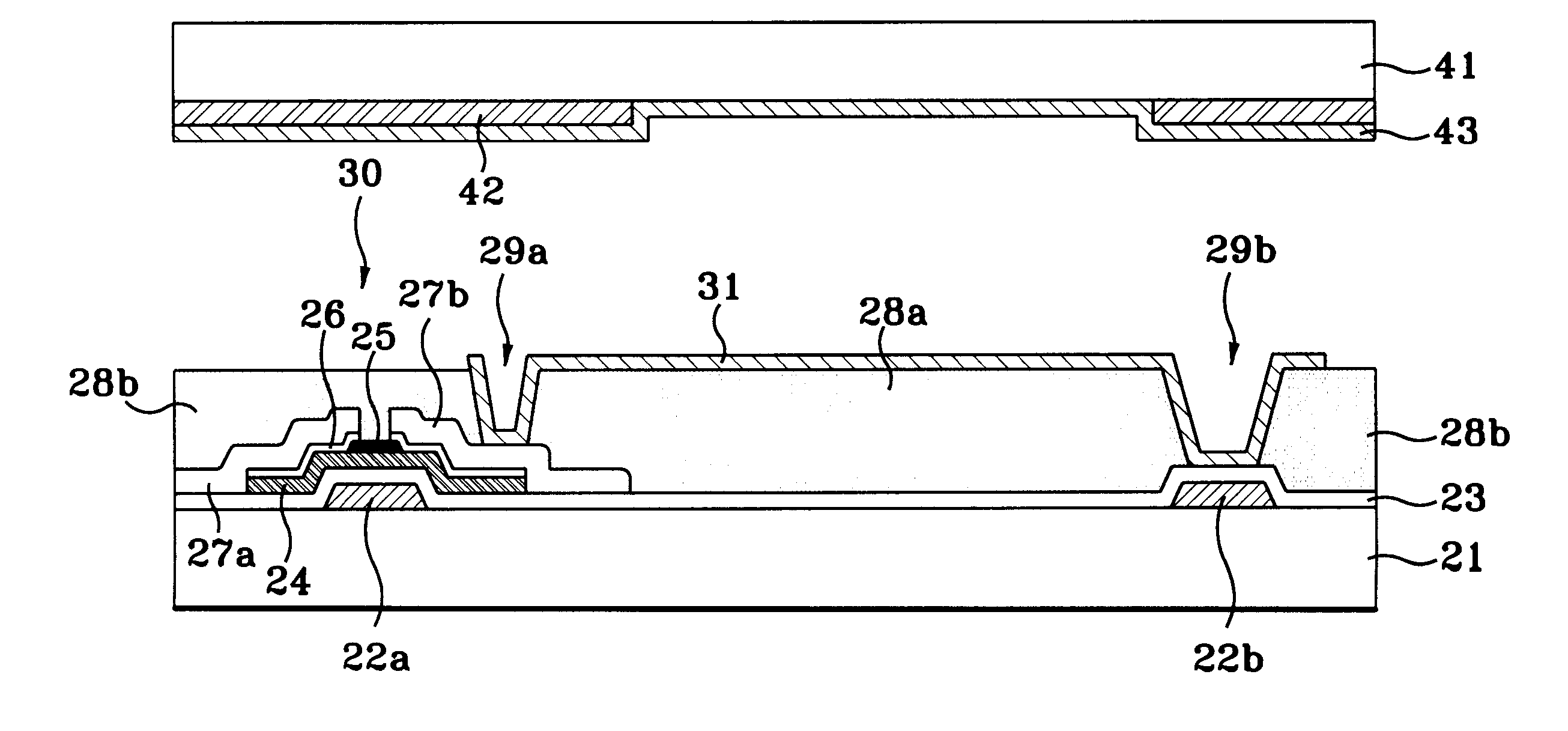
FIG. 2 illustrates a cross sectional view of a liquid crystal display according to a spirit of a present invention. On a portion of a lower substrate 21 an etch stopper inverse staggered type TFT 30, a switching device, is disposed. A storage electrode 22b is arranged on the same plane as a gate 22a of the TFT 30 and separated therefrom. Color filter layers 28a, 28b are arranged on the entire surface of the lower substrate 21 having the TFT 30. The color filter layer 28b covering the TFT 30 corresponds to the passivation layer 9 of FIG. 1, protecting the TFT 30 from an outside contamination. The color filter layers 28a and 28b have contact holes 29a and 29b, thereby exposing a drain 27b of the TFT 30 and an insulating layer 23 positioned on the storage electrode 22b. The pixel electrode 31 is disposed on the color filter layer 28a including the contact holes 29a and 29b. The pixel electrode 31 is made of ITO. The pixel electrode 31 on the bottom surface of the contact hole 29b, the ...


PUM


Abstract

A color filter layer covering both a thin film transistor and a pixel electrode which are formed on a lower substrate. A portion of the color filter layer positioned on the thin film transistor serves a protection layer of the thin film transistor and the other portion of the color filter layer serves a conventional color filter layer which were conventionally formed on an upper substrate opposite to the lower substrate. Therefore, the process number for the LCD is decreased and thus the manufacturing cost of the LCD is reduced.

Description

1. Field of the InventionThe present invention is directed to a technique of a liquid crystal display, and more particularly to a thin film transistor liquid crystal display having an improved hue and a simple process thereof and a method for manufacturing the same.2. Description of the Related ArtIn general, a thin film transistor liquid crystal display includes a lower substrate, a thin film transistor, as a switching device, formed on the lower substrate, an upper substrate opposite to the lower substrate, a color filter of red, green and blue formed on the upper substrate and a liquid crystal sealed within a cavity defined by both substrates.FIG. 1 is a view showing a cross sectional view of the conventional thin film transistor liquid crystal display(TFT LCD).On a portion of a lower substrate 1 an etch stopper inverse staggered type thin film transistor 15 (E / S inverse staggered TFT) and on the other portion of the lower substrate 1 a pixel electrode 8 is disposed. The pixel el...

Claims


Application Information

Patent Timeline
IPC IPC(8): G02F1/13G02F1/1335G02F1/1343G02F1/136G02F1/1368
CPCG02F1/133512G02F1/1335G02F1/1343G02F1/136
Inventor CHOI, WOO HO
Owner BOE HYDIS TECH
Why Eureka
Try Eureka