Distributed photodiode structure

Inactive Publication Date: 2001-03-06
SILICON LAB INC
View PDF12 Cites 16 Cited by
  • Summary
  • Abstract
  • Description
  • Claims
  • Application Information

AI Technical Summary

Problems solved by technology

However, the photo-current collection region within an electric field, the drift region, in a PN photodiode is limited to the relatively thin depletion zone produced when the PN junction is reverse biased.
This thin drift region is much less efficient in the collection of photo-generated charge carrier pairs because most of the pairs are generated outside of depletion zone.
Also, the charge pairs generated outside of the depletion zone thermally diffuse to collection points margins of the P and N layers and into the depletion zone at a much slower relative speed resulting in slow photodiode performance.
In addition, the highly doped P and N regions result in high diode capacitance per unit area which further slows the performance of the photodiode.
Although a PIN photodiode outperforms a standard PN diode, the PIN photodiode structure cannot be easily manufactured by standard semiconductor processes wherein fabrication is typically performed on only one side of the semiconductor wafer 50.
As described above, it is difficult to integrate an efficient photodiode on the same semiconductor substrate as the transceiver circuit.

Method used


Image

  • Distributed photodiode structure
  • Distributed photodiode structure
  • Distributed photodiode structure

Examples


Embodiment Construction

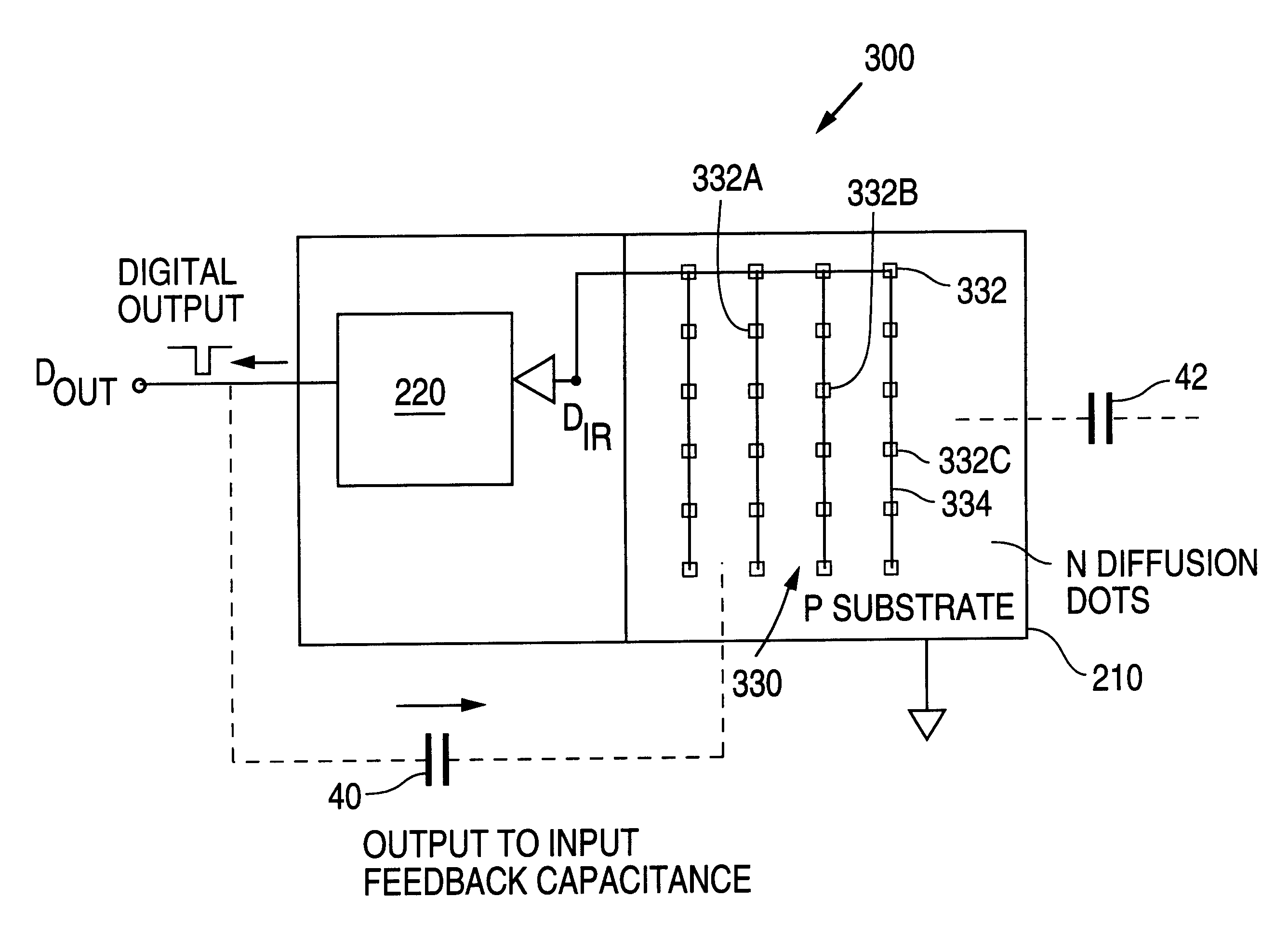
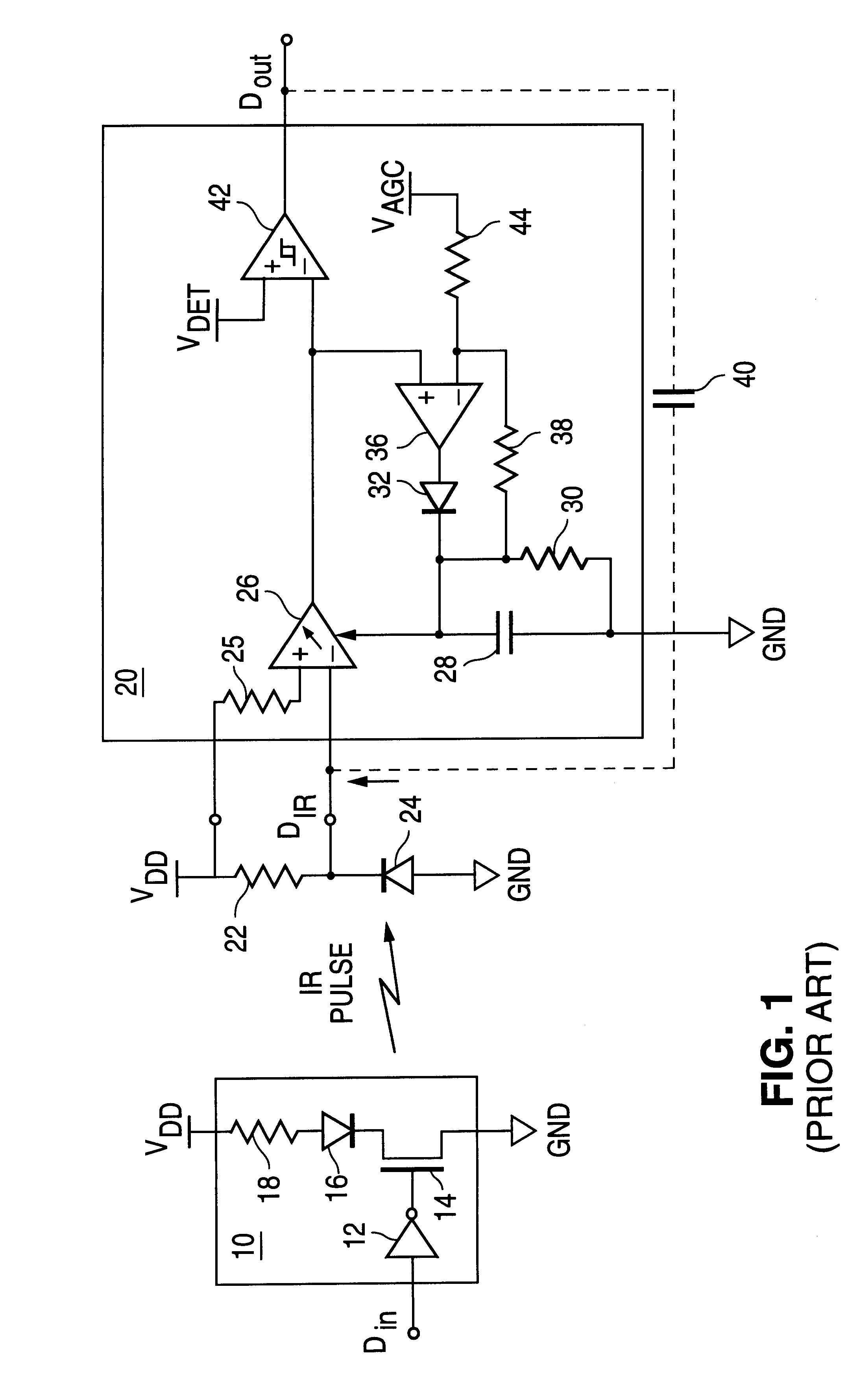
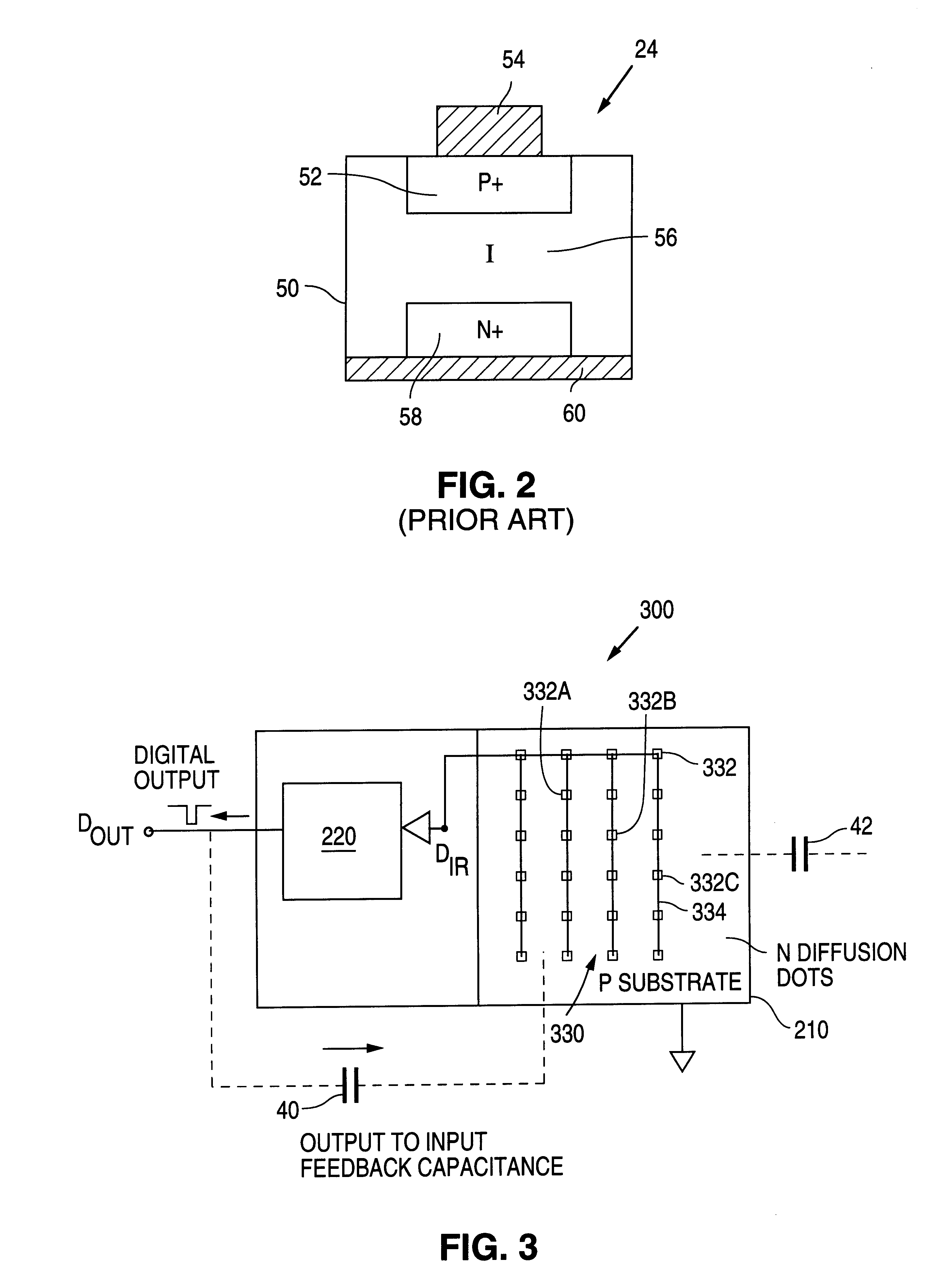
Because of the cost associated with assembling the transceiver module into a single package, it is desirable to integrate the photodiode and the receiver circuit on a single silicon substrate. However, constructing an IrDA receiver or transceiver with an integrated photodiode has typically not been either cost effective or sufficiently optically sensitive to have the range to meet, for example, the IrDA lowspeed specification.

In general, IrDA receivers typically use discrete photodiodes with areas of 3.4 to 25 square millimeters in order to produce the minimum signal level, typically 30 nA to 220 nA, required by the minimum detect threshold of an IrDA receiver at a range of 1 meter. A receiver or transceiver IC typically has an area of 2 to 10 square millimeters depending upon the IC fabrication process technology employed and the complexity of the circuit design.

Although PN photodiodes can be constructed using a standard IC fabrication process, the resulting photodiodes typically s...


PUM


Abstract

A distributed photodiode structure is shown having a plurality of diffusions formed in a uniform pattern on a first surface of a semiconductor substrate and interconnected by a plurality of connective traces. The diffusions are minimum geometry dots for a standard semiconductor fabrication process that are spaced apart from one another by an interval that is less than an average distance travelled by photo-generated carriers in the substrate before recombination. A conductive backplane is formed on a second surface of the semiconductor substrate to produce an inverted induced signal for noise cancelling.

Description

1. Field of InventionThe present invention relates to a photodiode which can be fabricated using standard semiconductor fabrication techniques.2. Description of the Related ArtInfrared wireless data communication is a useful method for short range (in the approximate range of 0-10 meters) wireless transfer of data between electronic equipment; such as, cellular phones, computers, computer peripherals (printers, modems, keyboards, cursor control devices, etc.), electronic keys, electronic ID devices, and network equipment. Infrared wireless communication devices typically have the advantages of smaller size, lower cost, fewer regulatory requirements, and a well defined transmission coverage area as compared to radio frequency wireless technology (i.e. the zone of transmission is bounded by physical walls and therefore more useful in an office environment). In addition, infrared wireless communication has further advantages with regard to reliability, electromagnetic compatibility, mu...

Claims


Application Information

Patent Timeline
IPC IPC(8): H01L31/103H01L31/102H01L31/0352H01L31/0248H01L31/02H04B10/152H04B10/158H01L31/10H04B10/02H04B10/04H04B10/06H04B10/10H04B10/14H04B10/26H04B10/43
CPCH01L31/02005H01L31/0352H01L31/103H04B10/114H04B10/40
Inventor HOLCOMBE, WAYNE T.
Owner SILICON LAB INC
Why Eureka
Try Eureka