Automated inspection system for metallic surfaces

a technology of automatic inspection and inspection system, applied in the direction of optically investigating flaws/contamination, measurement devices, instruments, etc., can solve the problems of high integration density, high manufacturing yield, and easy affecting of delicate metallurgical and chemical processes

Inactive Publication Date: 2001-03-06
GLOBALFOUNDRIES INC
View PDF9 Cites 110 Cited by
  • Summary
  • Abstract
  • Description
  • Claims
  • Application Information

AI Technical Summary

Problems solved by technology

The art of semiconductor manufacturing has become sufficiently advanced that extremely complex devices can be fabricated at high integration density and very high manufacturing yield.
In either case, the delicate metallurgical and chemical processes involved can be easily affected by contamination and other conditions which are not completely preventable and localized defects often occur.
Chip carriers, on the other hand, are subjected to inspection as well as functional testing prior to being populated with chips since many defect types which can occur in connections and pads cannot be detected by functional testing alone.
Multiple inspections by different operators are considered to be required since inspection efficiency of individual operators is low.
Further, the number of operators required for even modest production quantities engenders inconsistency in the inspection process.
It can be readily understood that such an inspection process is labor-intensive and costly.
The cost of such inspection thus adds significantly to the cost of the finished circuit packages while not insuring a maximal manufacturing yield.
With reflective white light inspection systems, some surface defects such as dishdowns (a substantial decrease in circuit trace height) may also be detected by such systems but these systems are not intended for more subtle surface imperfections and are inefficient and inaccurate when used for such a purpose.
Further, the cameras used in these systems are line scan cameras providing only a single pass during scanning and thus are of limited flexibility relative to illumination of the object being inspected.
In this regard, the metallic surface of a wirebond pad is very difficult to illuminate in a consistent manner and may have variable surface textures due to minor process fluctuations which obscure certai

Method used


Image

  • Automated inspection system for metallic surfaces
  • Automated inspection system for metallic surfaces
  • Automated inspection system for metallic surfaces

Examples


Embodiment Construction

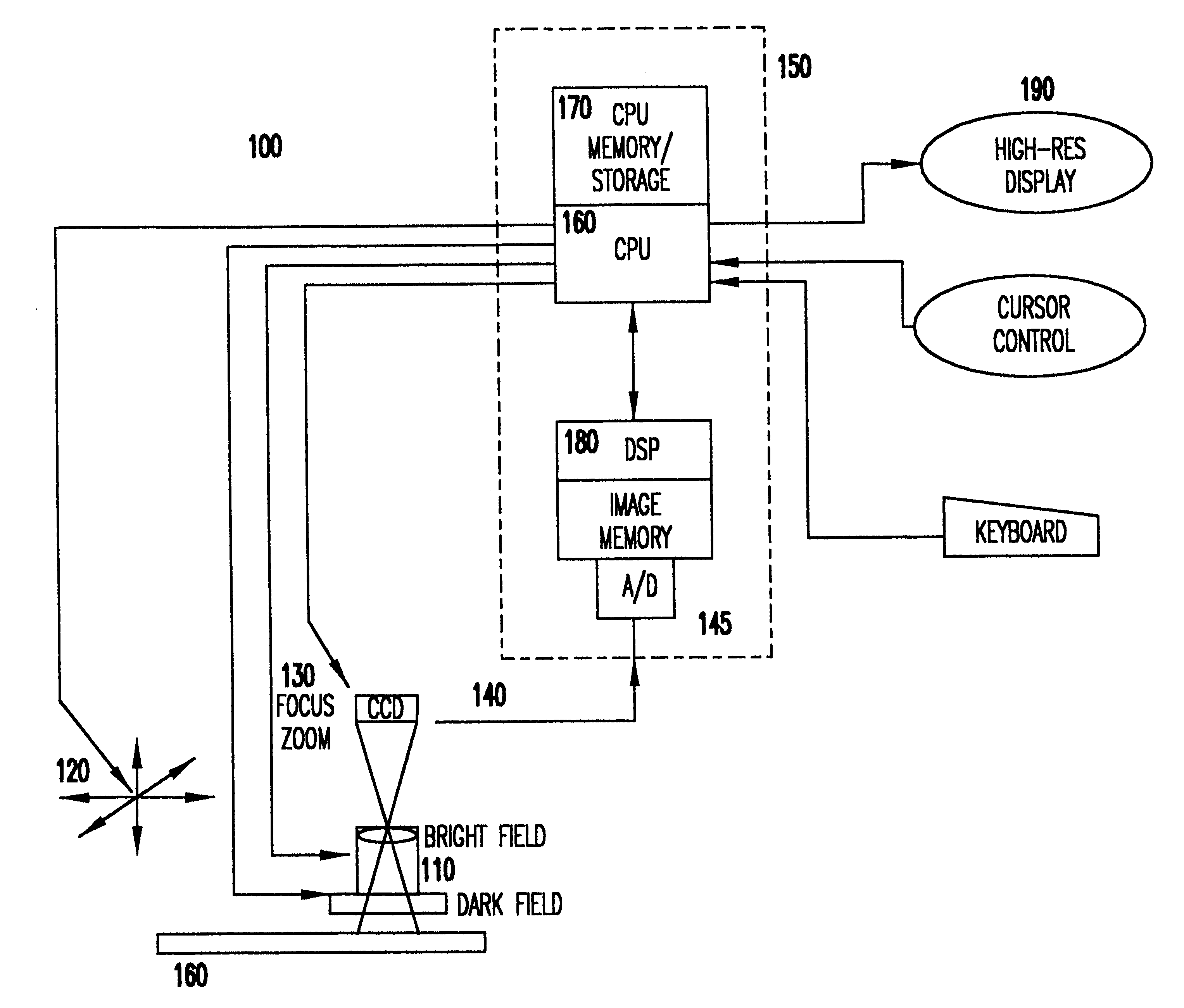
Referring now to the drawings, and more particularly to FIG. 1, there is shown a high-level block diagram of a preferred form 100 of the invention. While some features of FIG. 1 may be known in automated inspection systems not directed to or adapted for surface inspection, as alluded to above, and some individual elements are commercially available so that, as is preferred, the system can have a modular architecture which is easily reconfigurable for specific inspection tasks, the combination of elements depicted is, in fact, particularly adapted thereto. Further, at the level of abstraction represented in FIG. 1, the general organization of the invention may appear more similar to known systems than may, in fact, be the case, as will become evident from the following discussion. Accordingly, no portion of FIG. 1 is admitted to be prior art in regard to the present invention.

For example, all optical inspection systems, including known systems, require an arrangement 110 for illumina...


PUM


Abstract

An automated inspection system particularly adapted for detection and discrimination of surface irregularities of specularly reflecting and other materials, such as are employed in laminate chip carriers and printed circuit boards, includes an area scan image sensor allowing illumination sources to surround an area of a surface being inspected. The illumination source preferably provides either or both bright field and dark field illumination of the surface; developing generally complementary images of surface irregularities. A self-registering rules-driven process for developing inspection masks reduces alignment operations and improves performance. Image enhancement and morphological operations to detect surface irregularities are performed by digital signal processing, preferably using a dedicated vision processor. Masks screen potential defects to critical mounting and bonding surfaces accurately without requiring alignment of data or reference images to acquired images. Since potential defects are copied from acquired images and stored, verification of defects may be performed without further access to the inspected part and without removal of the part to another specialized apparatus, simplifying processing and increasing throughput and operator efficiency.

Description

1. Field of the InventionThe present invention generally relates to automated optical inspection (AOI) systems and, more particularly, to automated inspection systems suitable for end-of-line semiconductor component manufacture and packaging, especially for inspection of metallic wirebond surfaces used with laminated chip carriers.2. Description of the Prior ArtThe art of semiconductor manufacturing has become sufficiently advanced that extremely complex devices can be fabricated at high integration density and very high manufacturing yield. Increases in chip integration density has required similar increases in chip carrier complexity and feature density to complement the advantages of reductions in connection length achieved on individual chips. In either case, the delicate metallurgical and chemical processes involved can be easily affected by contamination and other conditions which are not completely preventable and localized defects often occur. For this reason, sophisticated ...

Claims


Application Information

Patent Timeline
IPC IPC(8): G01N21/956G01N21/88
CPCG01N21/95684G01N2021/8825
Inventor CLARK, JR., JOHN C.GILLIS, EARLE W.MAJKA, CHRISTOPHER J.SEWARD, MATTHEW F.WESTGATE, MICHAEL M.
Owner GLOBALFOUNDRIES INC
Why Eureka
Try Eureka