Semiconductor imaging device

a technology of electromagnetic radiation and imaging device, which is applied in the direction of light-controlled amplifiers, color televisions, television systems, etc., can solve the problems of reducing the resolution of the overall imaging surface, limiting the practical size of monolithic detectors to a few square centimeters, and eliminating inactive areas

Inactive Publication Date: 2001-03-27
SIEMENS HEALTHCARE GMBH +1
View PDF10 Cites 40 Cited by
  • Summary
  • Abstract
  • Description
  • Claims
  • Application Information

AI Technical Summary

Problems solved by technology

However, limitations in ASIC CMOS technology limit the practical size of monolithic detectors to a maximum area of a few square centimeters.
However, it has been a major problem to eliminate the inactive areas between the active imaging areas of adjacent detector devices.
Such inactive areas decrease the resolution of the overall imaging surface below the excellent resolution usually associated with each individual detector, and cause blind regions.
This arrangement addresses the problem of inactive area between adjacent detector de...

Method used


Image

  • Semiconductor imaging device
  • Semiconductor imaging device
  • Semiconductor imaging device

Examples


Embodiment Construction

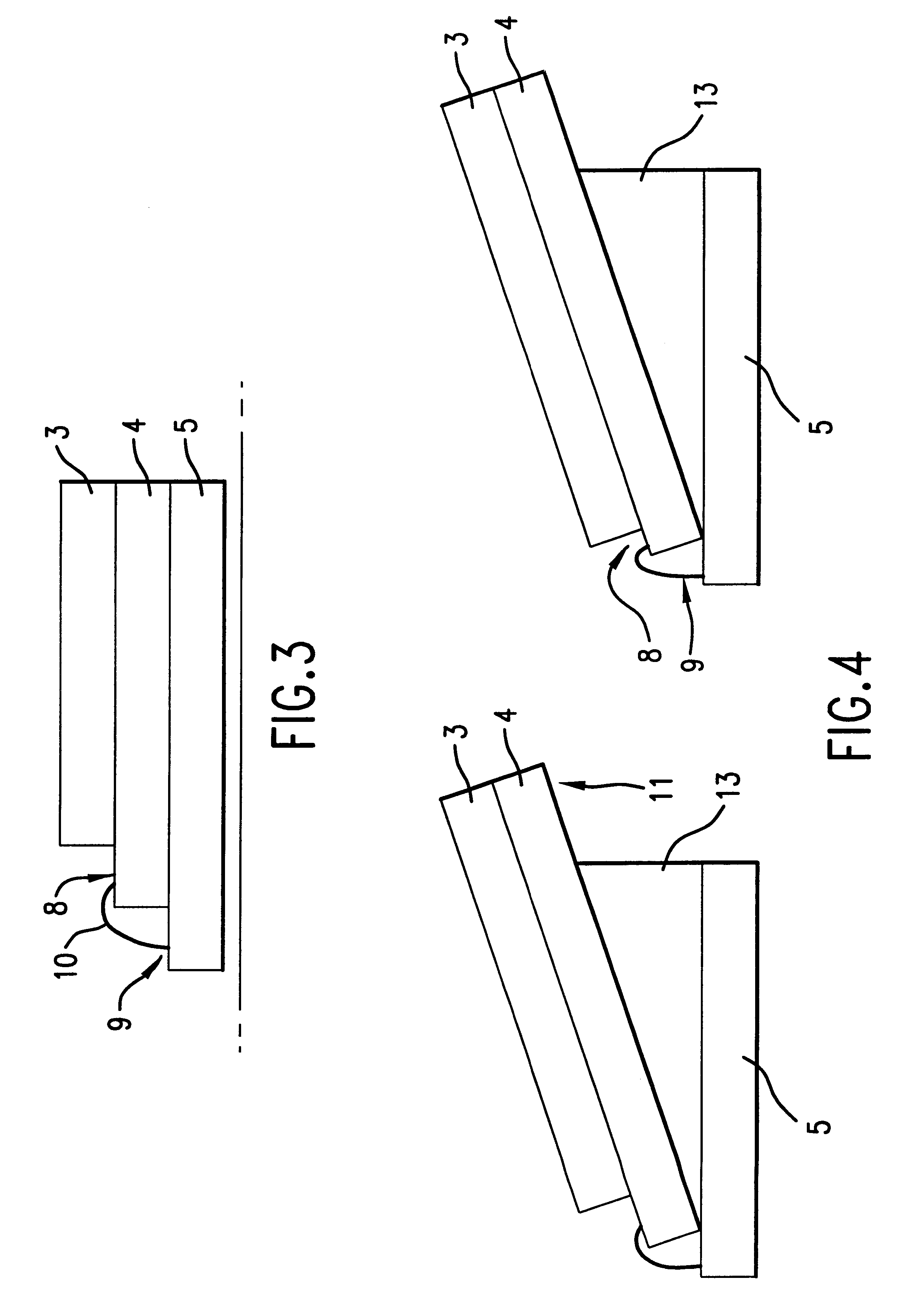
Embodiments of the invention are now described by way of example only with reference to the accompanying further drawings.

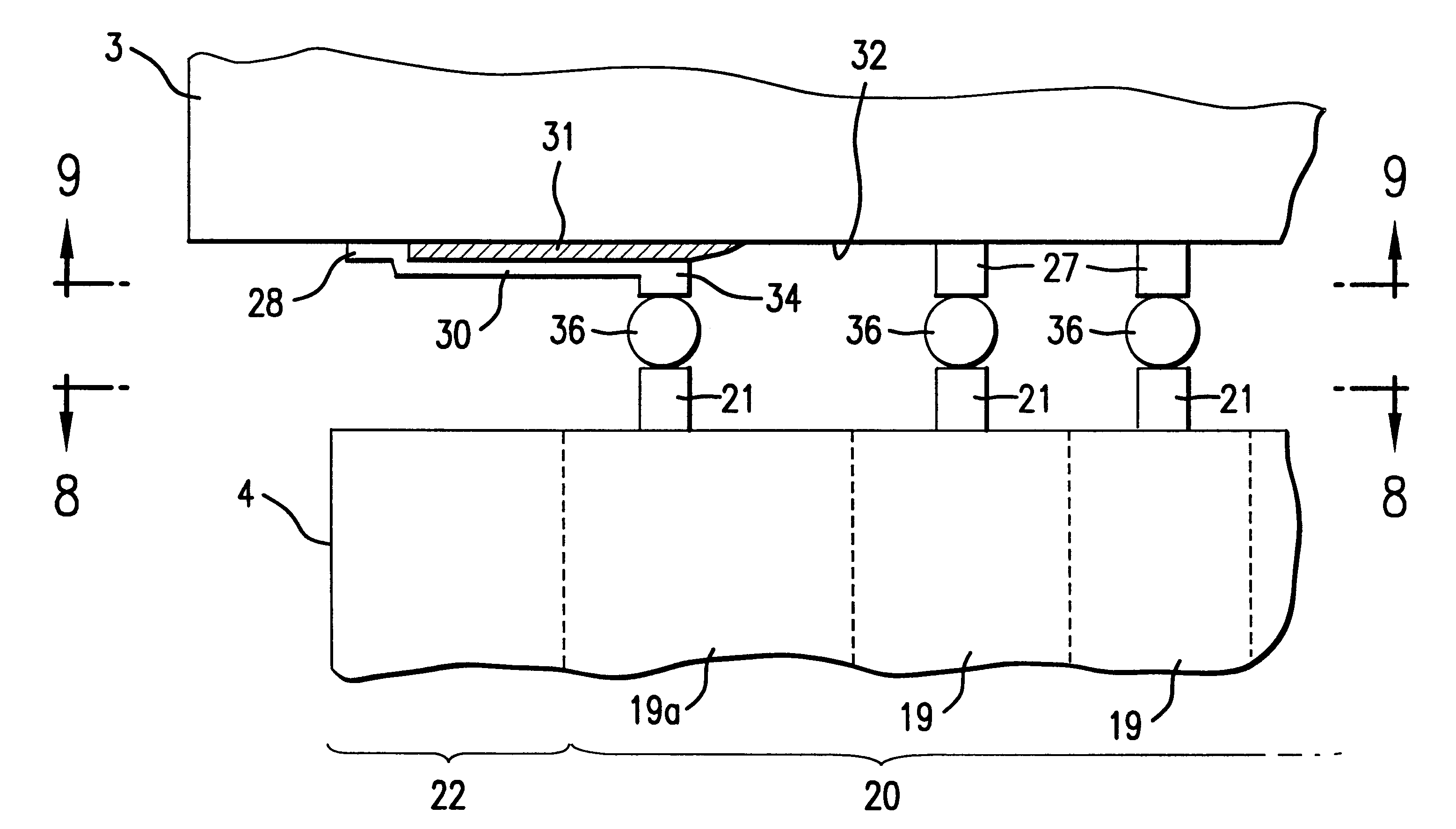
Referring to FIGS. 7, 8 and 9, the detector includes a semiconductor detector substrate 3 exposable to incident radiation and arranged in front of a read out substrate in the form of an integrated circuit 4. In FIG. 8, the position of the detector substrate 3 is indicated by a broken line; in FIG. 9, the position of the integrated circuit is indicated by a broken line. The detector substrate may be of any suitable material, for example, cadmium zinc telluride (CdZnTe), cadmium telluride (CdTe), lead iodide (PbI), gallium arsenide (GaAs), germanium (Ge), silicon (Si), or indium antinomide (InSb). In the present embodiment, CdZnTe is the preferred material.

The integrated circuit 4 includes a first region 20 which contains pixel cell readout circuits 19 with metal inputs 21, a second edge region 22 which contains additional circuitry such as control, decoding and mu...


PUM


Abstract

A semi-conductor imaging device, for example for x-ray imaging, uses a detector substrate exposable to incident radiation and having a plurality of charge collection contacts for collecting charge therefrom, the detector substrate being arranged in front of a readout substrate carrying or comprising readout circuitry, the readout substrate using a first region with a respective cell circuit coupled to each charge collection contact for receiving signals from the detector substrate, and a second region with further circuitry, and such that the charge collection contacts are arranged over both the first and second regions of the readout substrate. A conductive path connects each charge collection contact over the second region with a respective terminal for contacting an input of a cell circuit in the first region. The invention enables the part of the detector substrate overlying the additional circuitry to be used as active detection area.

Description

This invention relates to an imaging device, in particular to a semiconductor imaging device. The invention finds application to large area imaging, and is particularly suitable for X-ray imaging.BACKGROUND OF INVENTIONImaging devices are used in medical diagnosis, biotechnology or industrial non-destructive testing and quality control. Imaging is mostly carried out by means of ionizing radiation such as X-rays, gamma rays or beta rays. Radiation is detected by an imaging surface which need not be planar. Image formation is carried out either by viewing the two dimensional array representing the radiation intensity incident on the detector or by decoding and / or combining one or more sets of images (coded aperture imaging in nuclear medicine, computerized tomography).The traditional imaging device is cassette film. Other devices developed and utilized over the past 40 years include wire chambers, scintillating crystals or screens (e.g., sodium iodide Nal), BGO crystals, and digital i...

Claims


Application Information

Patent Timeline
IPC IPC(8): H01L27/146H01L31/02H04N5/32
CPCH01L27/14601H01L31/02002H04N5/32
Inventor SPARTIOTIS, KONSTANTINOS EVANGELOSPYYHTIA, JOUNI ILARICAO, TIELANG
Owner SIEMENS HEALTHCARE GMBH
Why Eureka
Try Eureka