
Optical disk, optical disk device, and method of reproducing information on optical disk

a technology of optical disk and optical disk, which is applied in the field of optical disk, optical disk device, and method of reproducing information on optical disk, can solve the problems of erroneous detection of address marks, erroneous bit shifts of "1" and difficulty in detecting the beginning of recording sector 103

Inactive Publication Date: 2001-03-27
PANASONIC CORP
View PDF24 Cites 38 Cited by
  • Summary
  • Abstract
  • Description
  • Claims
  • Application Information

AI Technical Summary

Problems solved by technology

This makes it difficult to detect the beginning of the recording sector 103 by the envelope.
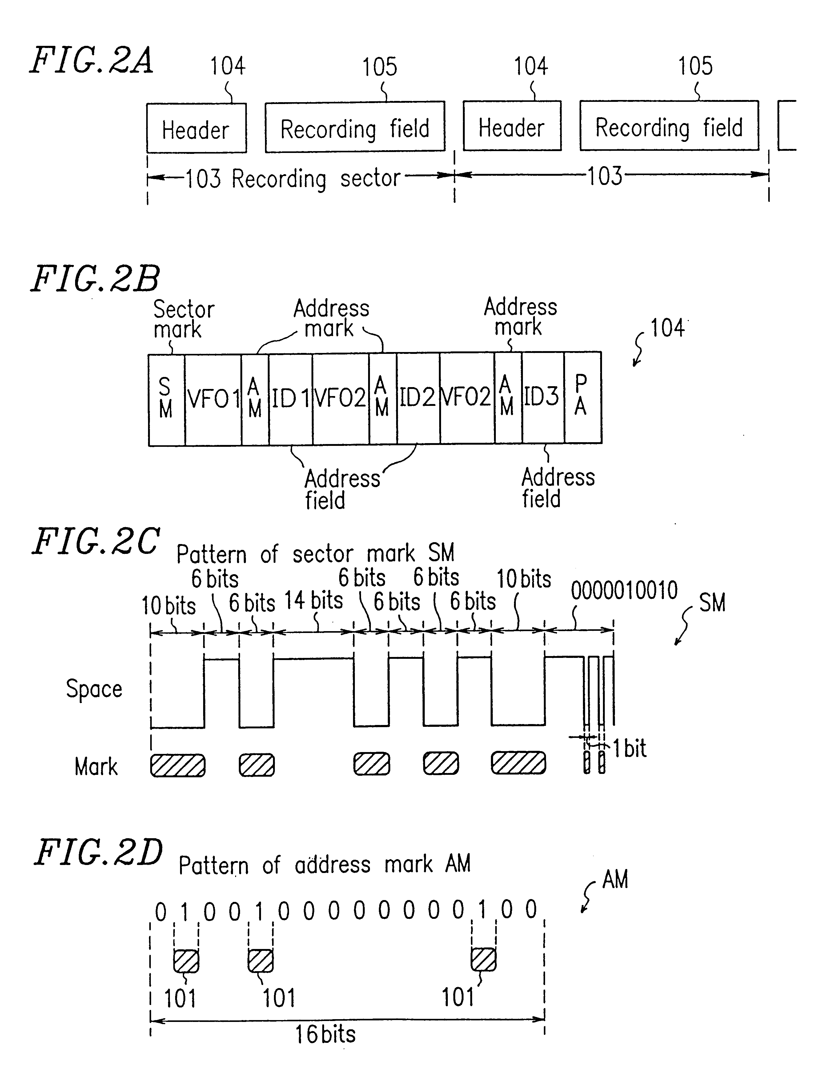
Moreover, when the above-described address mark AM is used, an erroneous detection of the address mark AM due to an erroneous bit shift of "1" may occur.
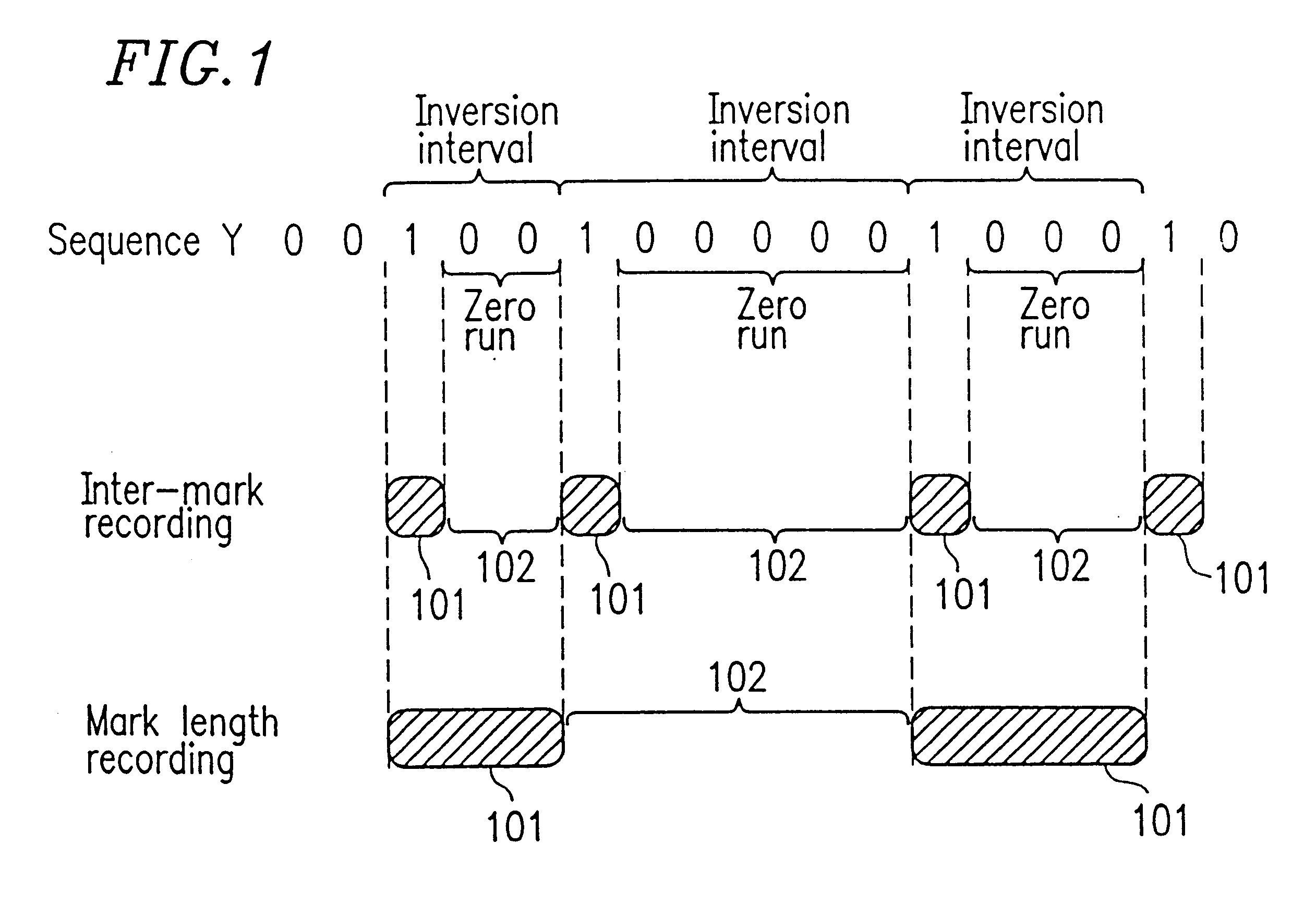
If "1" of the above (2,7) modulated pattern shifts by one bit, the resultant pattern is identical to the address pattern AM, which will cause erroneous detection.

Method used


Image

  • Optical disk, optical disk device, and method of reproducing information on optical disk
  • Optical disk, optical disk device, and method of reproducing information on optical disk
  • Optical disk, optical disk device, and method of reproducing information on optical disk

Examples


example 2

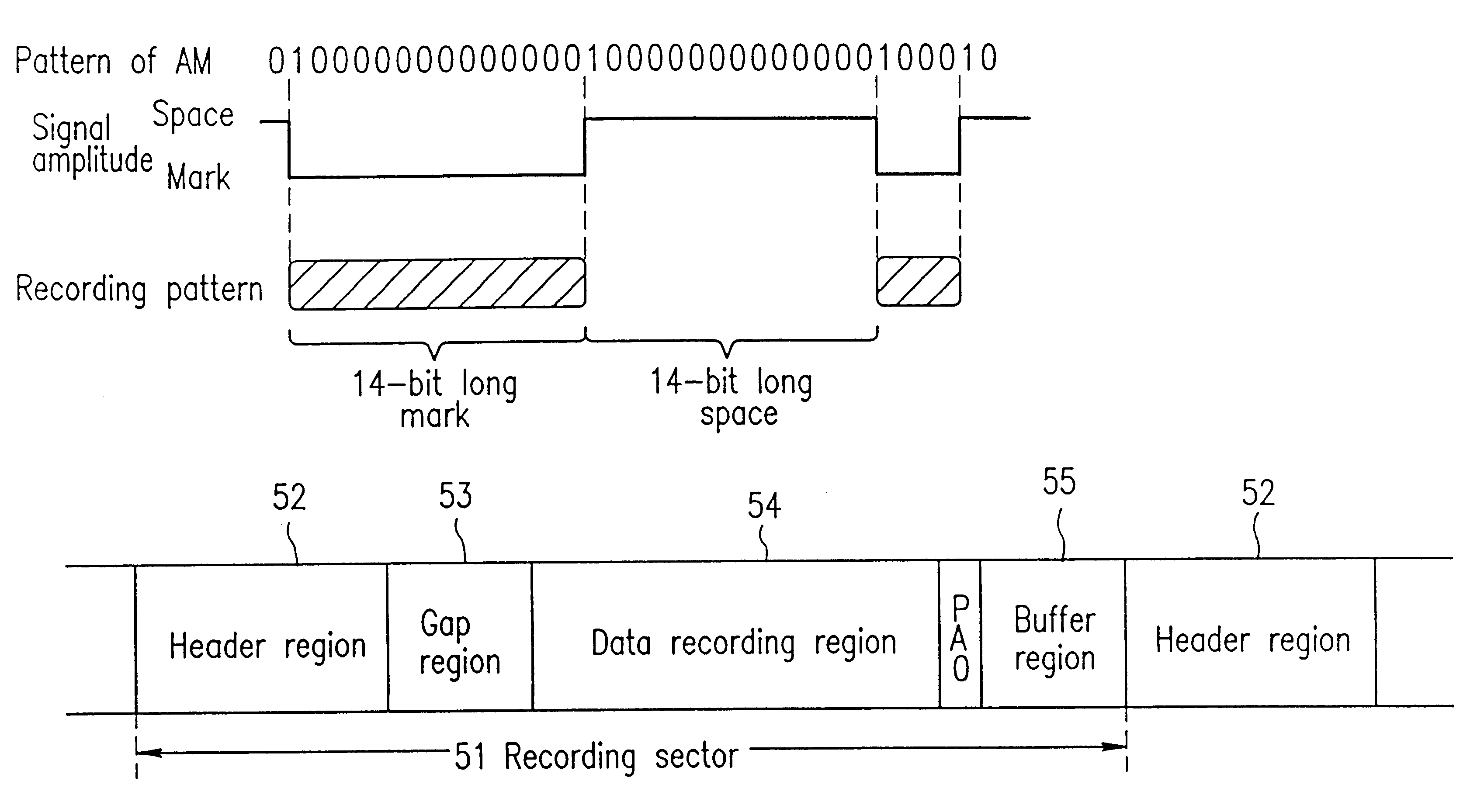
FIG. 17A is a view illustrating a format of a recording sector 51 of an optical disk of the second example according to the present invention. As shown in FIG. 17A, the recording sector 51 starts with a header region 52 where addressing information for reading address information is prerecorded. A gap region 53, a data recording region 54, a postamble PAO, and a buffer region 55 respectively follow the header region 52 in this order.

The gap region 53 has no data recorded thereon, but is used for power control of a semiconductor laser used for date recording / reproduction and the like, for example. The data recording region 54 is used to record user data. Redundant data such as an error correction code is added to the user data, to form digital data. The digital data is modulated using a run length limit code generated by use of a state machine. The modulated data is recorded on the data recording region 54 using the mark length recording. This run length limit code is called a state ...

example 3

FIG. 20A schematically illustrates an optical disk 201a of the third example according to the present invention. Referring to FIG. 20A, the optical disk 201a has tracks 201b formed on the surface thereof in a spiral shape. Each track 201b is divided into recording sectors 201c in accordance with a predetermined physical format. As shown in FIG. 20A, the recording sectors 201c are sequentially arranged in the circumferential direction to form one track 201b.

FIG. 20B illustrates a format of each recording sector 201c of the optical disk 201a of the third example according to the present invention. Referring to FIG. 20B, the recording sector 201c starts with a header region 202 where addressing information for reading address information is prerecorded. A gap region 203, a data recording region 204, and a buffer region 205 follow the header region 202 in this order. The gap region 203 has no data recorded thereon, but is used for power control of a semiconductor laser used for data rec...

example 4

FIG. 25A illustrates a format of a recording sector 61 of an optical disk of the fourth example according to the present invention. The recording sector 61 starts with a header region 62 where addressing information for reading address information is prerecorded. A gap region 63, a data recording region 64, a postamble 65, a guard data recording region 66, and a buffer region 67 follow the header region 62 in this order. The gap region 63 has no data recorded thereon, but is used for power control of a semiconductor laser used for data recording / reproduction and the like, for example. The data recording region 64 is used to store user data. Redundant data such as an error correction code is added to the user data, to form digital data. The digital data is modulated using a predetermined run length limit code, and recorded on the data recording region 64 using the mark length recording.

The postamble 65 indicates the end of the data recording region 64. The pattern of the postamble 65...


PUM

PropertyMeasurementUnit
widthaaaaaaaaaa
diameteraaaaaaaaaa
diameteraaaaaaaaaa

Abstract

The present invention is aimed at providing an optical disk, an optical disk device, and an optical disk reproduction method, for allowing for stable and efficient reading of address information. The optical disk includes a plurality of tracks each divided into a plurality of recording sectors. Each of the recording sectors includes a header region. The header region includes address information for identifying the position of the corresponding recording sector and address synchronous information for identifying the recording position of the address information for bit synchronization. The address information has been modulated using a run length limit code of a maximum inversion interval of Tmax bits (Tmax is a natural number), and the address synchronous information includes two patterns of which inversion interval is (Tmax+3) bits or more, so that the reproduced signal of the address synchronous information is distinguished from the reproduced signal of other information.

Description

The prevent invention relates to an optical disk, an optical disk device, and an optical disk reproduction method, for recording / reproducing digital signals.In recent years, optical disk devices have attracted attention as means for recording / reproducing a large capacity of data, and are under active technical developments for achieving higher recording density.Presently prevailing rewritable optical disks include spiral-shaped groove tracks composed of concave and convex portions (each having a width of about 50%) formed on a surface of a disk substrate at a pitch of 1 to 1.6 .mu.m. On the surface of the substrate, a thin film including a recording material (e.g., Ge, Sb, and Te in the case of a phase-change type optical disk) as a component is formed by a method such as sputtering. The disk substrate is fabricated in the following manner. First, a stamper is, produced from a prototype where concave grooves and pits for sector addresses and the like are formed by cutting by light b...

Claims


Application Information

Patent Timeline
Patent Type & Authority Patents(United States)
IPC IPC(8): G11B20/14G11B20/12G11B27/30G11B27/24G11B27/19G11B7/007
CPCG11B7/00718G11B7/00745G11B20/1217G11B20/1252G11B20/1426G11B27/19G11B27/24G11B27/3027G11B7/24082G11B2020/1232G11B2020/1267G11B2020/1274G11B2020/1287G11B2220/20G11B2220/216G11B2220/2537G11B20/1833
Inventor ISHIDA, TAKASHIGUSHIMA, TOYOJI
Owner PANASONIC CORP
Learn More