Method for fabricating a self aligned contact which eliminates the key hole problem using a two step spacer deposition

a technology of self-aligning contact and spacer deposition, which is applied in the direction of semiconductor devices, capacitors, electrical equipment, etc., can solve the problems of cell failure, space between adjacent conductive structures becoming narrower, and the dimension and die size continue to decreas

Inactive Publication Date: 2001-04-10
TAIWAN SEMICON MFG CO LTD
View PDF8 Cites 38 Cited by
  • Summary
  • Abstract
  • Description
  • Claims
  • Application Information

AI Technical Summary

Problems solved by technology

However, as device dimensions and die sizes continue to decrease for higher density, the space between adjacent conductive structures becomes narrower.
The surface of the sidewall spacers facing the contact opening become con

Method used


Image

  • Method for fabricating a self aligned contact which eliminates the key hole problem using a two step spacer deposition
  • Method for fabricating a self aligned contact which eliminates the key hole problem using a two step spacer deposition
  • Method for fabricating a self aligned contact which eliminates the key hole problem using a two step spacer deposition

Examples


second embodiment

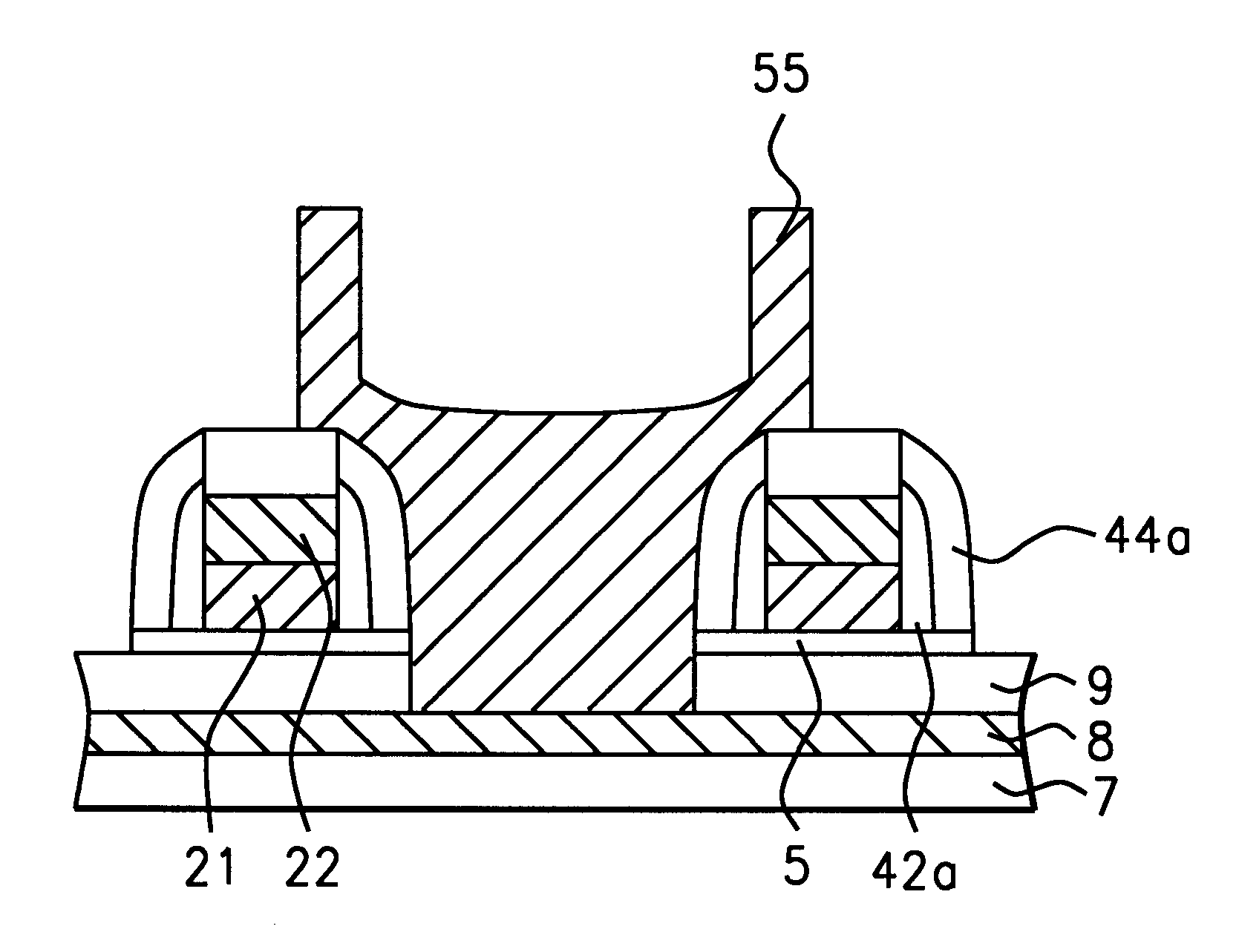
SiN First and Second Spacers

In an alternate embodiment of the invention, the first sidewall spacers (42A) and the second sidewall spacers (44A) are composed of silicon nitride. To prevent overetching of the hard mask during etching of the first sidewall spacer layer (42) to form the first sidewall spacers (42A), the hard mask is comprises a silicon nitride layer (31) with a silicon oxide layer (32) thereover.

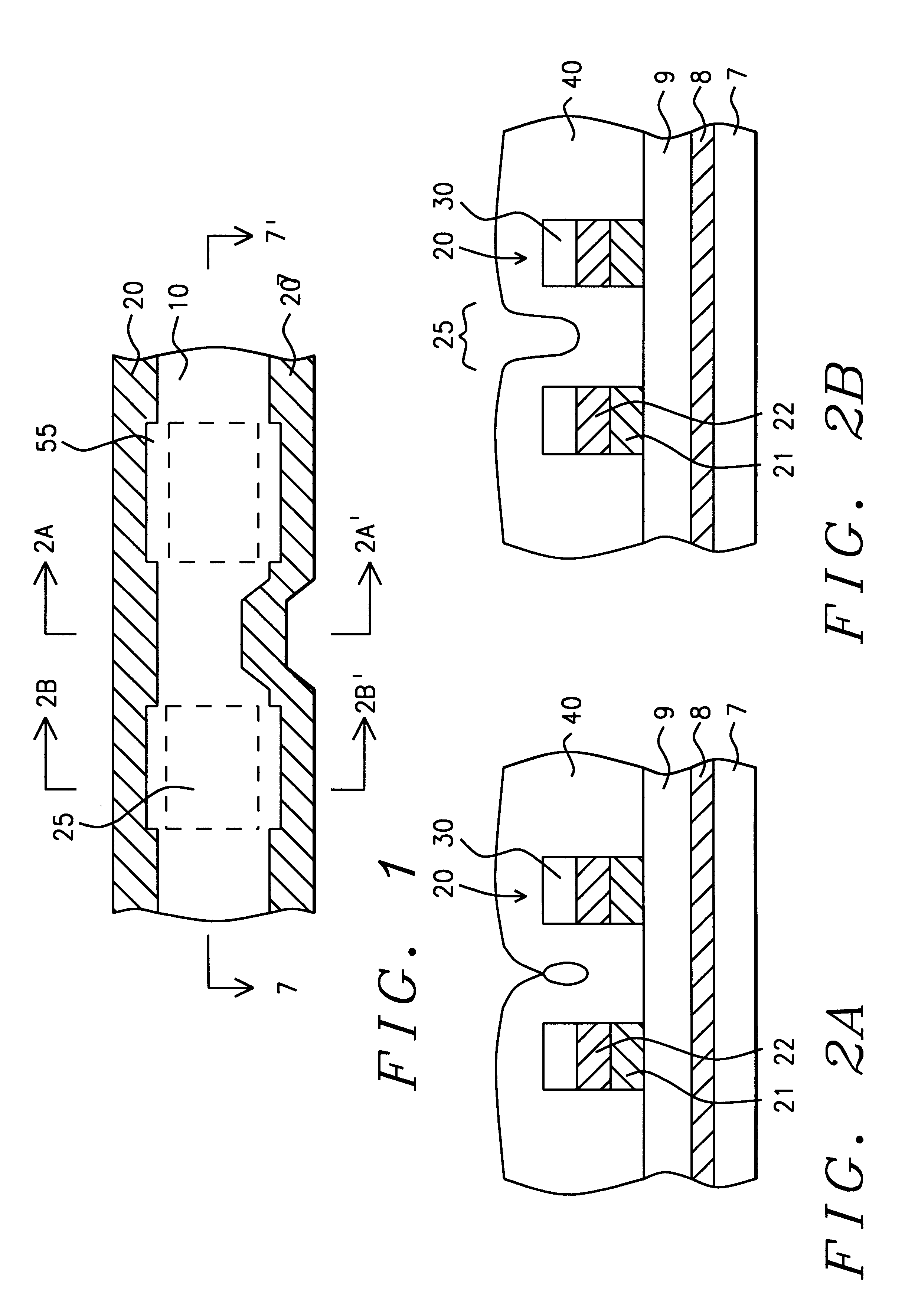
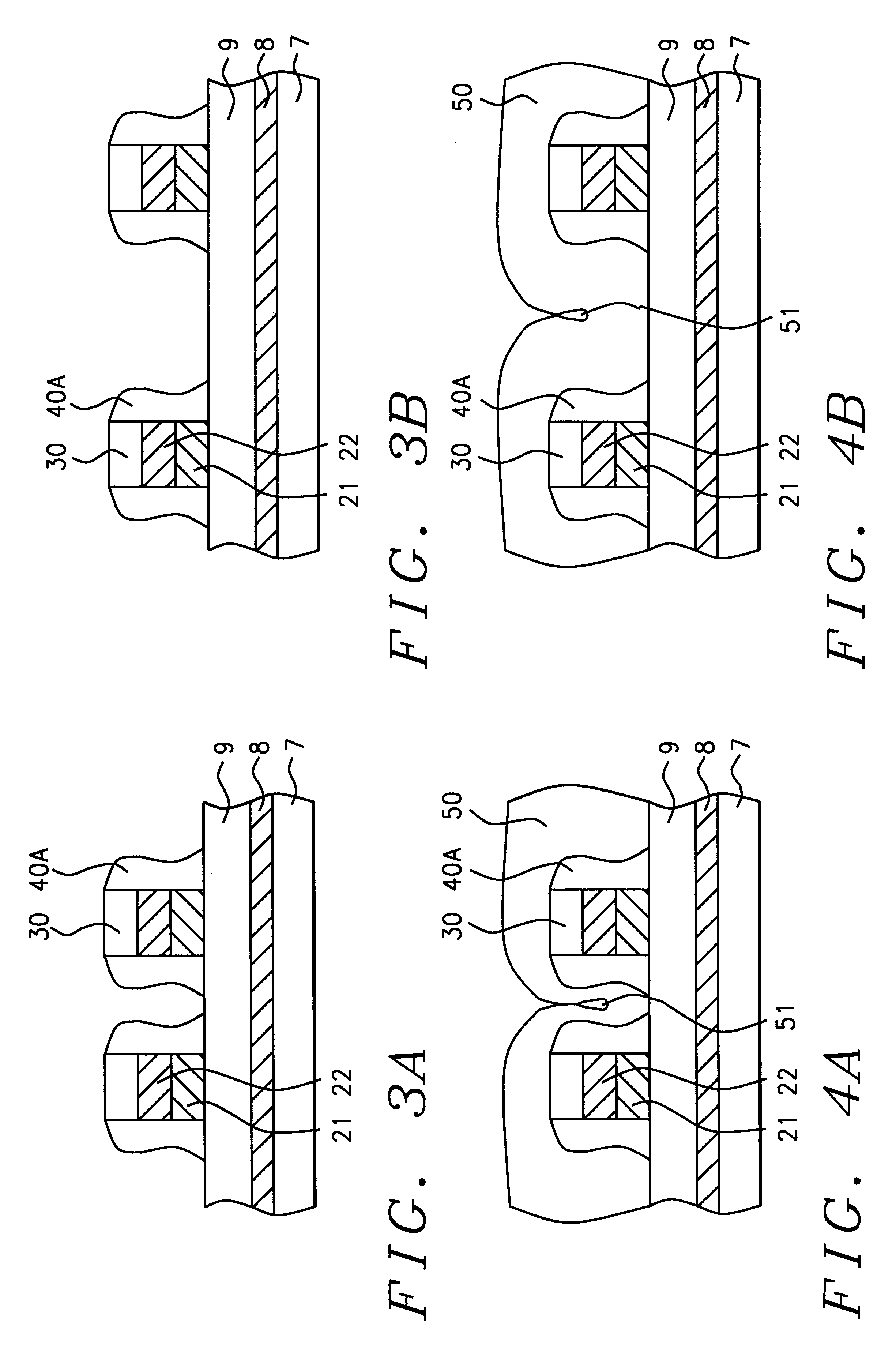
Referring to FIGS. 15A & 15B, the second preferred embodiment begins by providing a semiconductor structure (7) with a first device layer (8), a first interpolysilicon oxide layer (IPO-1) (9), and conductive structures (20) thereover, which are the same as the semiconductor structure (7), the first device layer (8), the first interpolysilicon oxide layer (IPO-1) (9),and the conductive structures (20) of the first embodiment in all respects. Like the semiconductor structure of the first embodiment, the semiconductor structure of the second embodiment can further comprise an etch ...


PUM


Abstract

This invention provides a method for forming a self aligned contact without key holes using a two step sidewall spacer deposition. The process begins by providing a semiconductor structure having a device layer, a first inter poly oxide layer (IPO-1), and a conductive structure (such as a bit line) thereover, and having a contact area on the device layer adjacent to the conductive structure. The semiconductor structure can further include an optional etch stop layer overlying the first inter poly oxide layer. The conductive structure comprises at least one conductive layer with a hard mask thereover. A first spacer layer is formed over the hard mask and the IPO-1 layer and anisotropically etched to form first sidewall spacers on the sidewalls of the conductive structure up to a level above the bottom of the hard mask and below the level of the top of the hard mask such that the profile of the first sidewall spacers are not concave at any point. A second spacer layer is formed over the first sidewall spacers and anisotropically etched to form second sidewall spacers, having a profile that is not concave at any point. A second inter poly oxide layer is formed over the second sidewall spacers, the hard mask, and the IPO-1 layer, whereby the second inter poly oxide layer is free from key holes. A contact opening is formed in the second inter poly oxide layer and the first inter poly oxide layer over the contact area. A contact plug is formed in the contact openings.

Description

1) Field of the InventionThis invention relates generally to fabrication of semiconductor devices and more particularly to a two step process for forming spacers in a self aligned contact process which eliminates the key hole problem in the IPO (inter-poly oxide) layer.2) Description of the Prior ArtThe use of self aligned contact (SAC) processes has resulted in higher performing, lower cost, and increased density semiconductor devices. A self aligned contact process spacers are formed on the sidewalls of conductive structures (such as gates and bit lines); and IPO layer is formed over these conductive structures; a contact opening is etched through the IPO; and a conductive layer is formed over the conductive structures and in the contact opening. However, as device dimensions and die sizes continue to decrease for higher density, the space between adjacent conductive structures becomes narrower. The surface of the sidewall spacers facing the contact opening become concave (overhan...

Claims


Application Information

Patent Timeline
IPC IPC(8): H01L21/02H01L21/70H01L21/60H01L21/8242
CPCH01L21/76897H01L27/10855H01L28/92H01L27/10885H01L28/91H10B12/0335H10B12/482
Inventor HUANG, KUO-CHINGYING, TSE-LIANGCHIANG, WEN-CHUAN
Owner TAIWAN SEMICON MFG CO LTD
Why Eureka
Try Eureka