Multi-layer registration control for photolithography processes

a photolithography and multi-layer technology, applied in semiconductor/solid-state device testing/measurement, semiconductor/solid-state device details, instruments, etc., can solve the problem of increasing the cost of each i

Inactive Publication Date: 2001-04-17
NXP USA INC
View PDF8 Cites 77 Cited by
  • Summary
  • Abstract
  • Description
  • Claims
  • Application Information

AI Technical Summary

Problems solved by technology

As the scribe grid increases,

Method used


Image

  • Multi-layer registration control for photolithography processes
  • Multi-layer registration control for photolithography processes
  • Multi-layer registration control for photolithography processes

Examples


Embodiment Construction

The ensuing detailed description provides preferred exemplary embodiment(s) only, and is not intended to limit the scope, applicability, or configuration of the present invention. Rather, the ensuing detailed description of the preferred exemplary embodiment(s) will provide those skilled in the art with an enabling description for implementing preferred exemplary embodiment(s) of the invention. It being understood that various changes may be made in the function and arrangement of elements without departing from the spirit and scope of the invention as set forth in the appended claims.

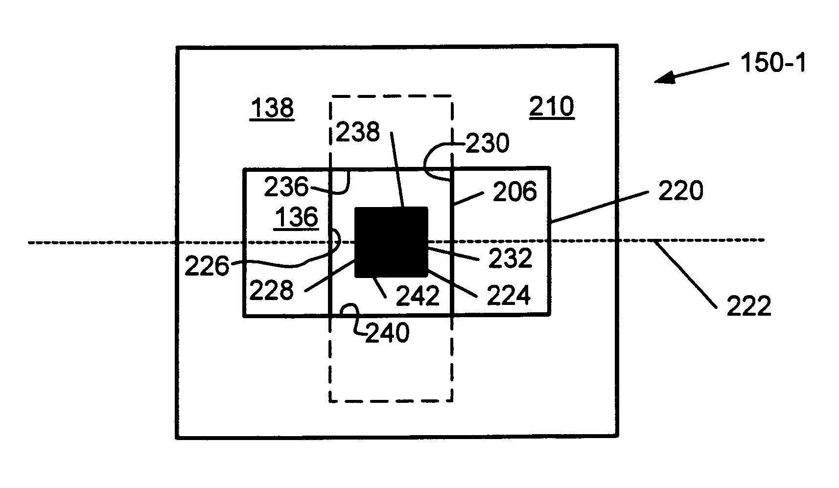
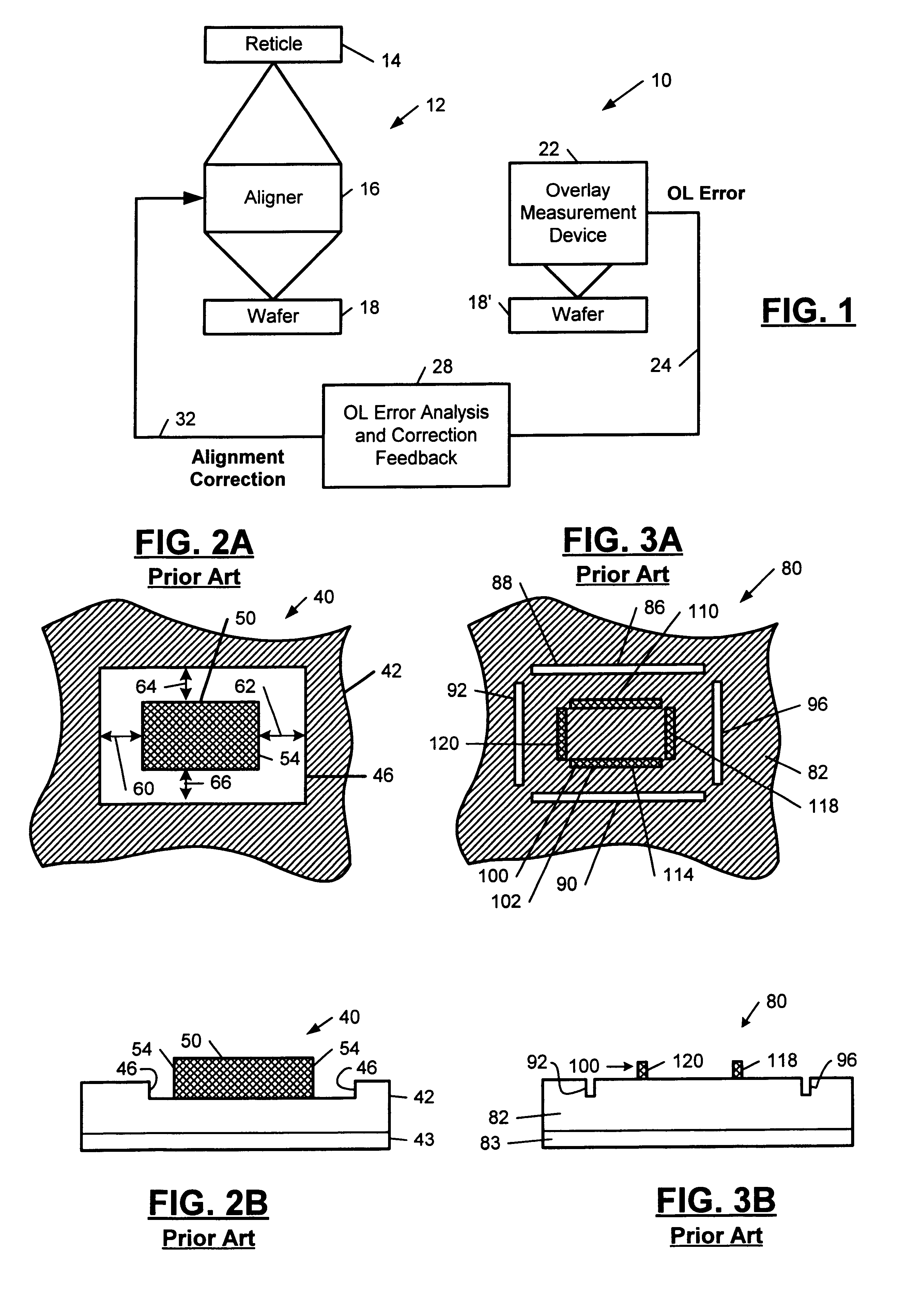
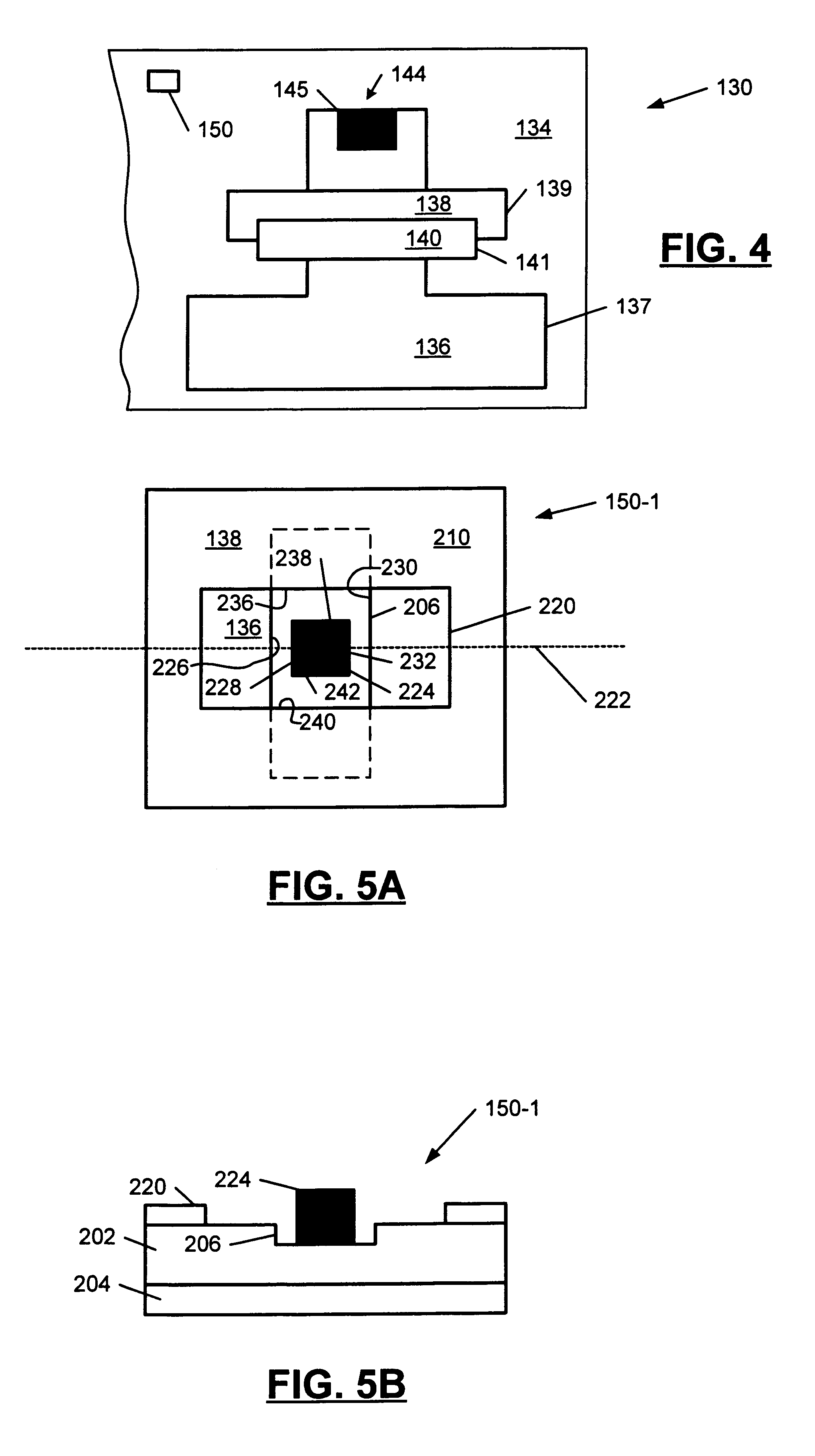
Referring to FIG. 1, a multi-layer registration control system 10 for a photolithography process is illustrated and includes a reticle-to-wafer aligner 12 that includes a reticle 14 and an aligner 16. During a photolithography process, one or more layers are printed on a wafer 18. As the layers are printed, one or more overlay marks are also printed in a scribe grid area. The overlay marks are used to ...


PUM


Abstract

A multi-level registration control system for a photolithography process includes a photolithography device that prints first, second and third layers on a wafer. A first overlay mark defines overlay errors in a first direction between the first and third layer. The first overlay mark also defines overlay errors between the second and third layers. An overlay measurement device measures the overlay errors and generates an overlay signal. A feedback controller is connected to the overlay measurement device and the photolithography device. The feedback controller receives the overlay error signal and generates and transmits an alignment correction signal to the photolithography device. The first overlay mark is a box-in-box overlay mark or a frame-in-frame overlay mark. By providing a single overlay mark to align three layers, the multi-layer overlay control system reduces scribe grid area and saves useful silicone surface area.

Description

1. FIELD OF THE INVENTIONThe present invention relates to photolithography processes, and more particularly, to methods and apparatus for multi-layer registration control in a photolithography process.2. BACKGROUND INFORMATIONIn a typical integrated circuit (IC) manufacturing process, a silicon wafer goes through many levels of processing to form the IC. Following a photoprocessing layer, designed circuit patterns are printed on multiple layers of a wafer surface to form the IC. Each layer must be aligned with a prior layer for the IC to operate properly. An overlay controller is generally employed to achieve alignment of two layers within the IC. The accuracy of the overlay controller directly impacts the yield of the IC manufacturing process. As a minimum feature size of the IC shrinks, the tolerance of the overlay controller becomes correspondingly smaller.Conventional overlay controllers for photolithography processes typically employ a reticle-to-wafer aligner, a stepper, or a ...

Claims


Application Information

Patent Timeline
IPC IPC(8): G03F7/20H01L21/66H01L23/544
CPCG03F7/70633H01L22/34H01L22/12
Inventor CHEN, GONGCOLCLASURE, JR., ROBERT D.PAULSON, WAYNE M.
Owner NXP USA INC
Why Eureka
Try Eureka