Optical information recording and reproducing apparatus for multiple layer recording medium

a technology of optical information and recording medium, which is applied in the direction of light beam reproducing, instrumentation, disposition/mounting of heads, etc., can solve the problems of manufacturing yield being unsatisfactory, manufacturing optical disks can be deformed, and only a single information layer in the structure of recording information encounters limitations

Inactive Publication Date: 2001-05-01
PANASONIC CORP
View PDF40 Cites 24 Cited by
  • Summary
  • Abstract
  • Description
  • Claims
  • Application Information

AI Technical Summary

Problems solved by technology

Although employment of the foregoing methods enables the recording capacity per unit area to be somewhat enlarged, a structure having only a single information layer for recording information encounters a limitation when the recording density is intended to be raised.
Thus, there arises a problem in that the manufacturing yield has been unsatisfactory.
In a case where the substrate 211 is made of a resin, change in the environmental temperature or in the humidity sometimes raises a problem in that the manufactured optical disk can be deformed or an error occurs in reproducing the signals.
Moreover, an apparatus of a type for reproducing information signals from a plurality of information layers has a problem in that the servo operation becomes instable due to an influence of light reflected by an information layer other than the subject information layer.
In particular, if a resin material is employed as the material of the substrates and if the substrates are formed by the injection molding method, the substrates can become deformed, such as warped, after being allowed to stand for a long time depending upon the molding conditions or the like.
Moreover, change in the environment temperature or humidity causes the substrates to be considerably deformed.
A main issue in the foregoing case lies in that convergence of the light beam 7 to an information layer which is out of the tolerance .DELTA.Wd of the thickness of the base results in a spherical aberration being generated and thus sufficient convergence of light spots being inhibited.
The foregoing phenomenon occurs in a case where a thin separation layer cannot easily be obtained when the separation layer 5 is formed or in a case where the accuracy of the thickness of the separation layer 5 is unsatisfactory.
The reason for this is that if a photodetector having the light receiving surface divided into two sections is used, then an operation of obtaining a servo signal from a subject information layer encounters the problem of the servo signal being distorted because a portion of light reflected by other information layers is made incident upon the photodetector.
Although reduction in the area of the light receiving portion of the photodetector enables the distortion of the servo signal to be inhibited, another problem arises is that a range for pulling focusing is excessively limited.
ace. Therefore, the focus error signal is distorted and, therefore, a focal-point positional error dF oc
e area. Thus, the operation becomes unstable if the recording medium is warped or has an irregularity on its
Therefore, error voltage is generated in the focus error signal or the tracking error signal due to interference between the information layers or change in the thickness of the separation layer when the servo operation is performed.

Method used


Image

  • Optical information recording and reproducing apparatus for multiple layer recording medium
  • Optical information recording and reproducing apparatus for multiple layer recording medium
  • Optical information recording and reproducing apparatus for multiple layer recording medium

Examples


example 2

(Example 2)

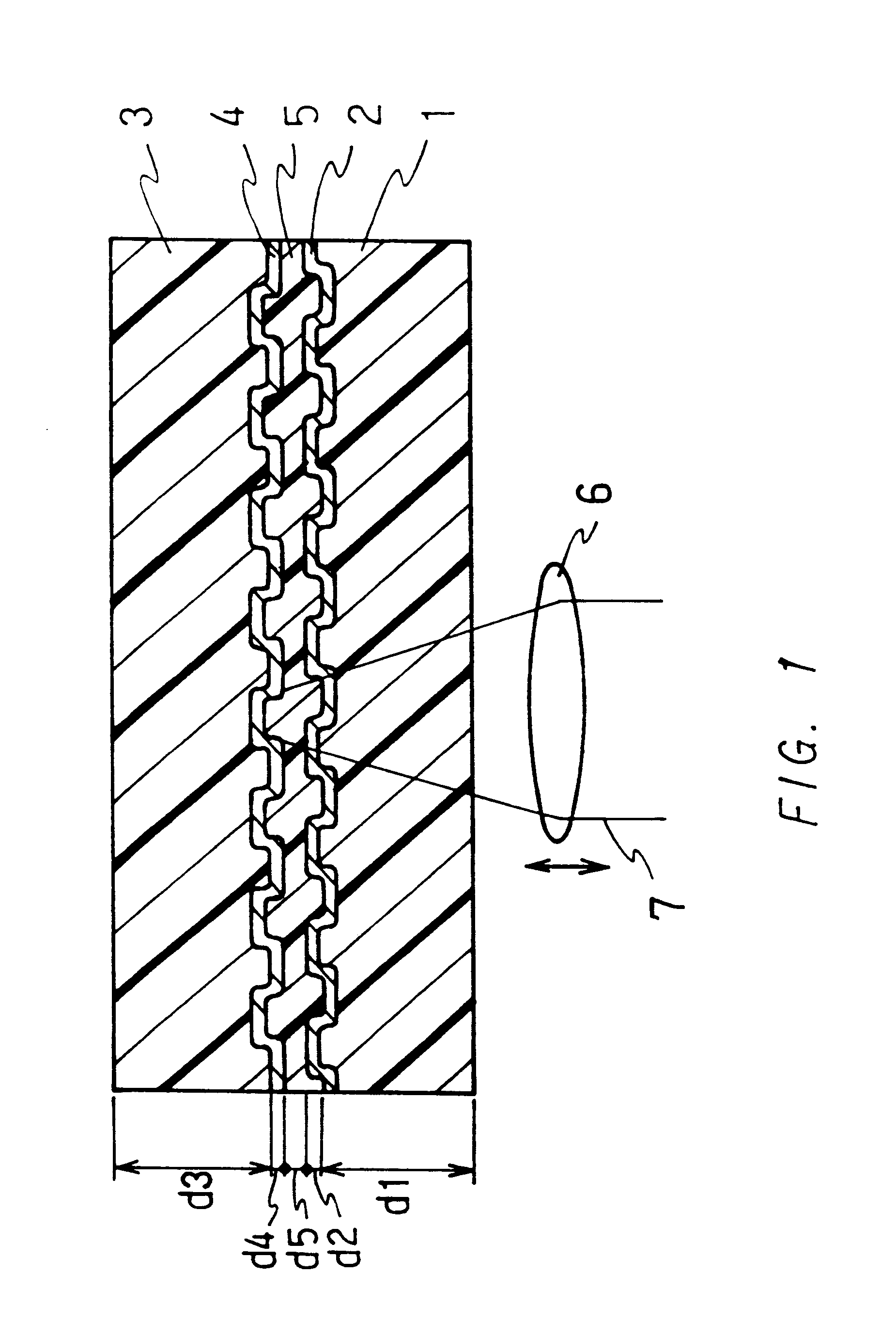
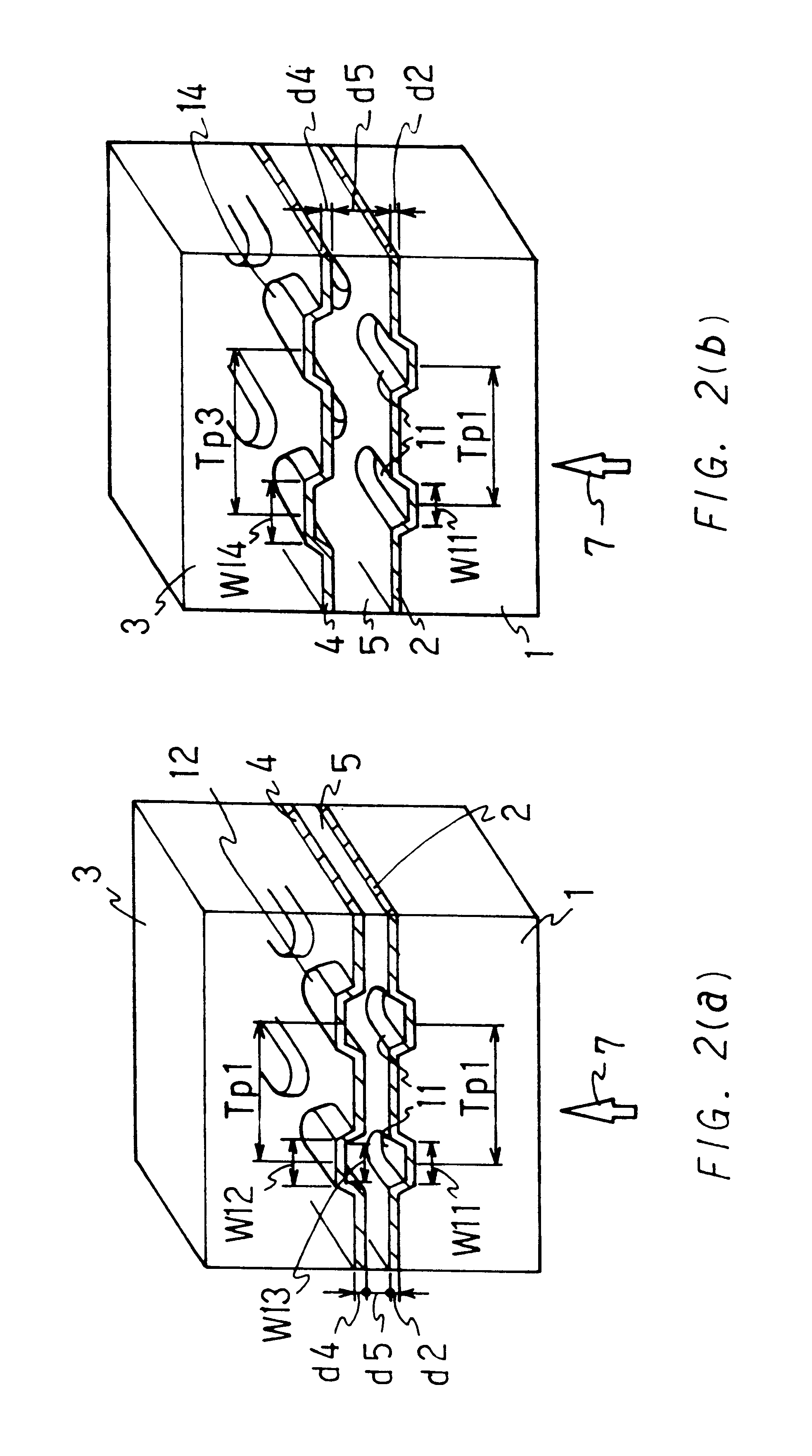
A structure of a recording medium capable of forming information more densely will now be described. Similarly to Example 1, polycarbonate resin was employed to form the first and second substrates 1 and 3, and a mold having a surface comprising information pits was used to perform injection molding so that the first and second substrates 1 and 3 were manufactured. The first substrate 1 had a thickness of 0.58 mm and comprised, on the surface thereof, information pits arranged such that the shortest pit length was 0.5 .mu.m, the pit depth was 90 nm and the track pitch was 0.8 .mu.m. On the first substrate 1, there was formed an Au layer having a thickness of 11 nm by a sputtering method so that the first information layer 2 was formed.

The second substrate 3 had the same thickness as that of the first substrate 1, the second substrate 3 having information pits in the same form as those of the first substrate 1. To make the direction of the spirals of the first substrate 1 ...

example 3

An example of a recording medium having four information layers as shown in FIG. 5 will now be described. Similarly to Example 1, polycarbonate resin was employed to form the first to fourth substrates 58, 60, 63 and 65, and a mold having a surface comprising information pits was used to perform injection molding so that the first to fourth substrates 58, 60, 63 and 65 were manufacture. Each of the first and third substrates had a thickness of 0.58 mm and comprised, on the surface thereof, information pits arranged such that the shortest pit length was 0.5 .mu.m, the pit depth was 90 nm and the track pitch was 0.8 .mu.m. On each of the first and third substrates 58 and 63, there was formed an Au layer having a thickness of 11 nm by a sputtering method so that the first and third information layers 59 and 64 were formed.

Each of the second and fourth substrates 60 and 65 had a thickness of 0.4 mm, which was smaller than that of each of the first and third substrates 58 and 63, in orde...

example 4

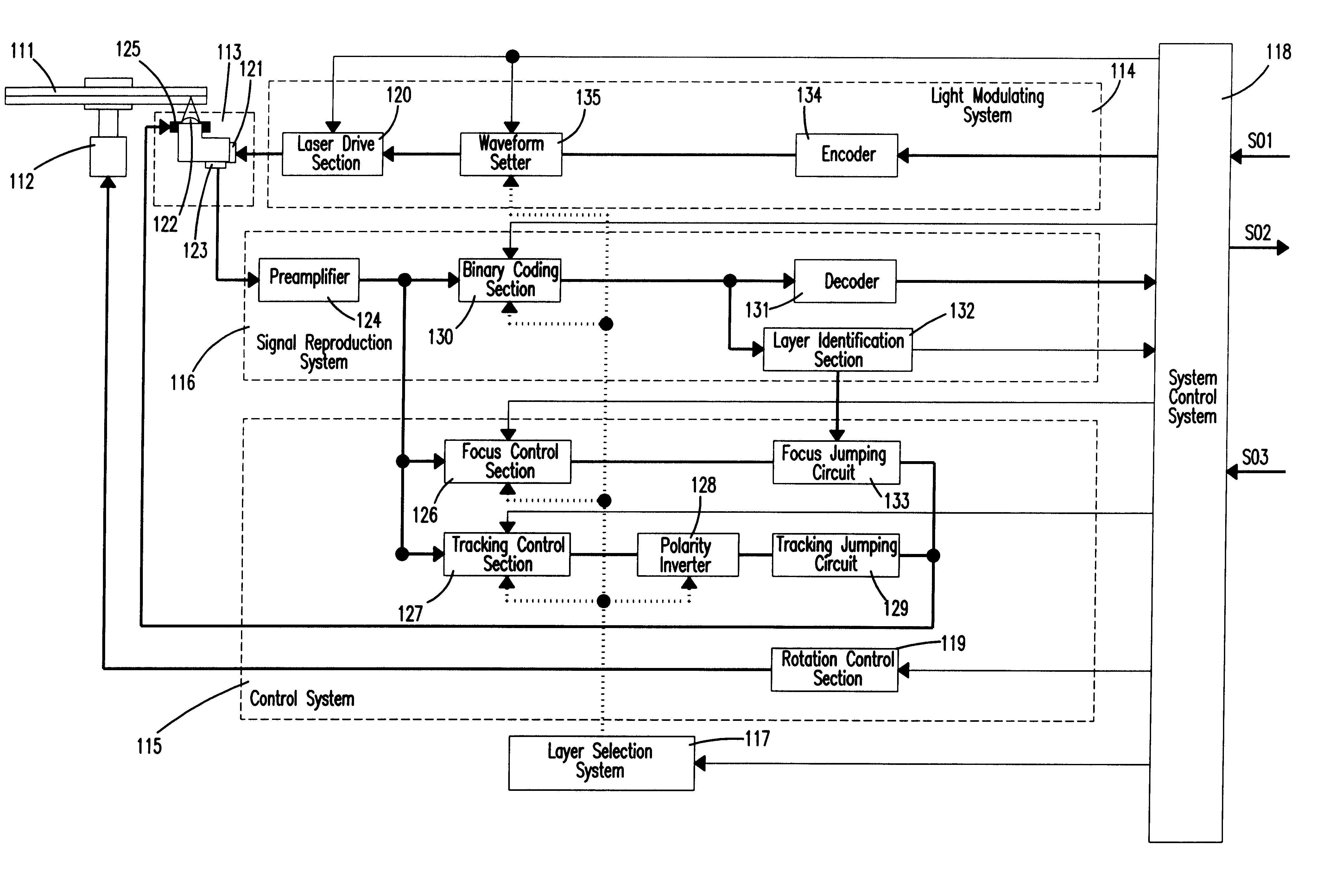
The specific structure of the optical information recording medium shown in FIG. 18 and recording and reproducing operations with the foregoing medium will now be described.

The first substrate 31 was made of polycarbonate resin and having, on the surface thereof, information pits formed in accordance with EFM modulation to correspond to information signals. The thickness d1 of the first substrate 31 was 0.58 mm and the diameter was 120 mm. The information pits formed on the surface of the first substrate 31 were arranged in such a manner that the shortest length of the pit of the pits formed on its surface was 0.44 .mu.m, the pitch depth was 90 nm and the track pitch was 0.74 .mu.m. A ZnS layer having a thickness of 40 nm was formed on the surface of the first substrate 31 by the sputtering method so that the first information layer 32 was formed.

The second substrate 33 was made of polycarbonate resin and had guide grooves for tracking light beams on the surface thereof. The second ...


PUM

PropertyMeasurementUnit
reflectanceaaaaaaaaaa
thicknessaaaaaaaaaa
thicknessaaaaaaaaaa

Abstract

In an optical information recording medium having at least two information layer, guide grooves for tracking or sample pits or information pits corresponding to information signals are formed on a surface of a first substrate. A first information layer formed by a thin line for reflecting a portion of a light beam made incident on the first substrate and permitting penetration of a portion of the light beam is formed on a surface of the first substrate. Guide grooves for tracking or information pits corresponding to information signals are formed on a surface of a second substrate. A second information layer having a reflection higher than that of the first information layer is formed on a surface of the second substrate. Between the first information layer and the second information layer, there is formed a transparent separation layer for positioning the first information layer and the second information layer to be spaced a predetermined distance apart from each other.

Description

The present invention relates to an optical information recording medium capable of reproducing information signals or recording and reproducing information signals by using light beams, a manufacturing method therefor, a manufacturing apparatus therefor and an optical information recording and reproducing apparatus making use thereof, and more particularly to an optical information recording medium having a multilayer structure including a plurality of information layers, a manufacturing method therefor, a manufacturing apparatus therefor and an optical information recording and reproducing apparatus making use therefor.DESCRIPTION OF THE PRIOR ARTHitherto, an optical information recording medium has been known which is capable of optically recording information signals or reproducing recorded information signals and which is formed into an optical disk, an optical card or the like. In general, the foregoing recording medium uses a semiconductor laser unit as a light source. By irr...

Claims


Application Information

Patent Timeline
Patent Type & Authority Patents(United States)
IPC IPC(8): B29C65/48G11B7/26G11B7/09G11B7/13G11B7/085G11B7/24G11B11/105G11B11/00G11B7/007G11B7/243G11B7/244G11B7/254G11B7/256
CPCB29C65/7811B29C66/452B32B37/1054B32B38/1841G11B7/08511G11B7/0901G11B7/0908G11B7/131G11B7/133G11B7/24G11B7/24038G11B7/24085G11B7/26B29C65/00B29C65/4845B29C65/782B29L2017/005B32B2429/02G11B7/007G11B7/0912G11B7/0916G11B7/094G11B7/0941G11B7/243G11B7/244G11B7/254G11B7/256G11B11/10586B29C65/7847B29C65/4815B29C65/4835B29C65/1406B29C65/7835B29C66/1122B29C66/71B29C66/723B29C66/73341B29C66/8322B29K2995/0027B29K2033/12B29K2069/00G11B7/2403
Inventor NISHIUCHI, KENICHINAGATA, KEN'ICHIAKAHIRA, NOBUO
Owner PANASONIC CORP
Why Eureka
Try Eureka