Current sensing in vacuum electron devices

a vacuum electron and current sensing technology, applied in the field of vacuum electron devices, can solve the problem that the technique is not suitable for controlling individual beam current in such a devi

Inactive Publication Date: 2001-05-22
INT BUSINESS MASCH CORP
View PDF12 Cites 3 Cited by
  • Summary
  • Abstract
  • Description
  • Claims
  • Application Information

AI Technical Summary

Problems solved by technology

However, this technique is not suitable for controlling individual beam current in such a device because the individual beam currents are effectively summed at the anode.

Method used


Image

  • Current sensing in vacuum electron devices
  • Current sensing in vacuum electron devices
  • Current sensing in vacuum electron devices

Examples


Embodiment Construction

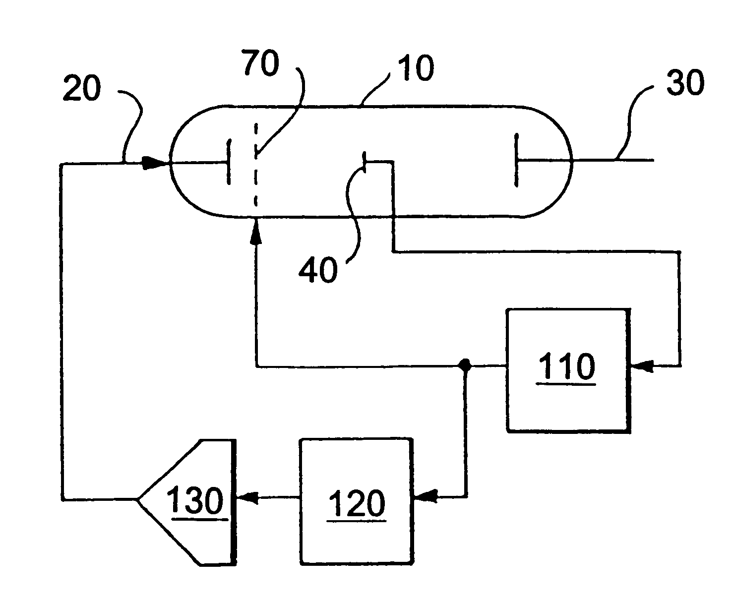
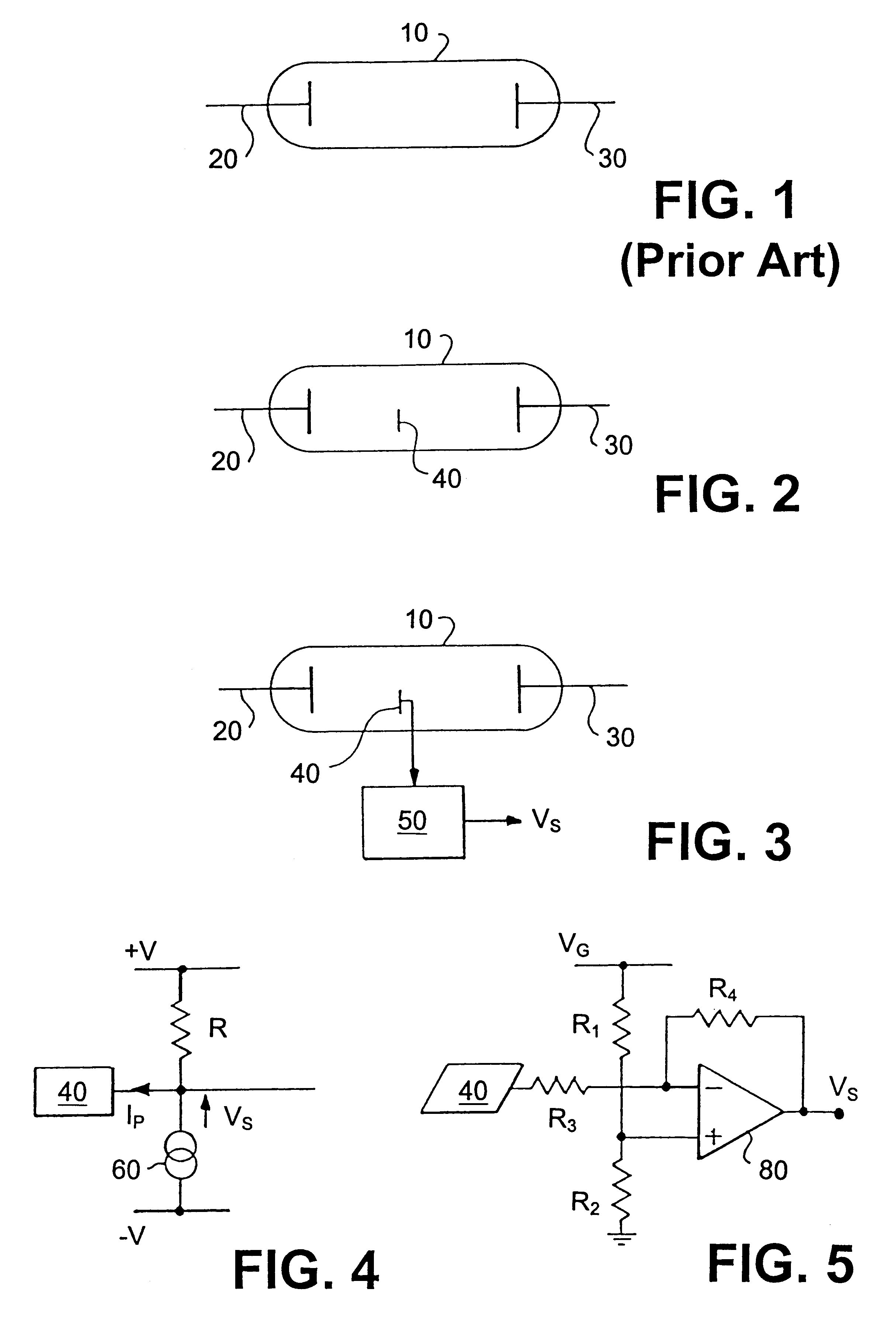
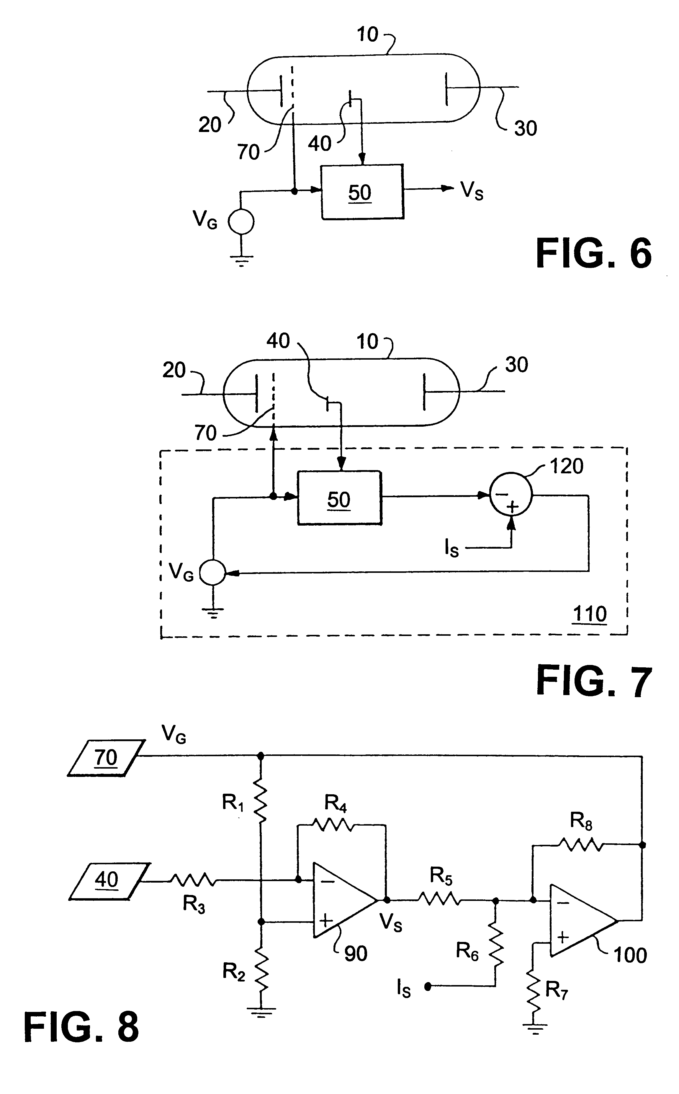
Referring to FIG. 1, an example of a simple vacuum electron device is a diode comprising an evacuated tube 10 containing an anode 30 and a cathode 20. In operation, the anode 30 is held at a potential greater than or equal to that applied to the cathode 20. Electrons released from the cathode 20 thus pass through the evacuated tube 10 to the anode 30. The anode current is defined by the number of electrons striking the anode 30.

The current flowing in the diode may be determined by measuring the current flowing into the cathode 20. A disadvantage with this approach is that the cathode may not be 100 percent efficient in electron conversion. Also, there is no certainty that all electrons leaving the cathode 20 will inevitably strike the anode.

The current flowing in the diode may alternatively be determined by measuring the current flowing from the anode 30. This approach is practical provided that the entire anode current is carried in a single electron beam. If the anode current is d...


PUM


Abstract

A vacuum electron device comprises an evacuated envelope containing a cathode for supplying electrons to form an electron beam, an anode spaced from the cathode for receiving the electron beam, and a sensor electrode located between the cathode and the anode.

Description

1. Field of the InventionThe present invention generally relates to vacuum electron devices and particularly relates to electron current sensing in vacuum electron devices.2. Background DescriptionA conventional vacuum electron device comprises an cathode and anode contained in an evacuated envelope. In operation, the cathode is held at a negative potential relative to the anode. Electrons are emitted from the cathode. The potential difference between the cathode and the anode accelerates the emitted electrons from the cathode towards the anode in a beam. A beam current thus flows between the anode and the cathode. In some conventional vacuum electron devices, such as cathode ray display tubes (CRTs), one or more grid electrodes are disposed between the cathode and the anode. In operation, a control voltage is applied to each of the one or more grid electrode(s). The control voltage imposes an electrostatic force on the electron beam. The electron beam current can be adjusted by adj...

Claims


Application Information

Patent Timeline
Patent Type & Authority Patents(United States)
IPC IPC(8): H01J29/00H01J29/58H01J29/98H01J61/02H01J61/56H01J29/68H01J7/00H01J37/24H01J19/00H01J7/44H01J37/02H01J19/82H01J29/02H01J1/00H01J31/12
CPCH01J7/44H01J19/82H01J29/68H01J29/98H01J37/243H01J61/56
Inventor BEETESON, JOHNKNOX, ANDREW RAMSAY
Owner INT BUSINESS MASCH CORP
Why Eureka
Try Eureka