Method of interconnecting electronic components using a plurality of conductive studs

a technology of conductive studs and electronic components, applied in the field of electronic components, can solve the problems of affecting the reliability of the resulting electronic module, affecting the reliability of the electronic module, and affecting the quality of the electronic component,

Inactive Publication Date: 2001-07-10
IBM CORP
View PDF9 Cites 213 Cited by
  • Summary
  • Abstract
  • Description
  • Claims
  • Application Information

AI Technical Summary

Problems solved by technology

Traditional methods of joining using solder ball arrays may become difficult with such dense circuitry.
With connection densities reaching about 150 .mu.m or below, it becomes difficult to clean such fluxes.
Without effective flux cleaning, underfill materials which are used to enhance reliability of the resulting electronic module run the risk of delaminating.
Th...

Method used


Image

  • Method of interconnecting electronic components using a plurality of conductive studs
  • Method of interconnecting electronic components using a plurality of conductive studs
  • Method of interconnecting electronic components using a plurality of conductive studs

Examples


Embodiment Construction

)

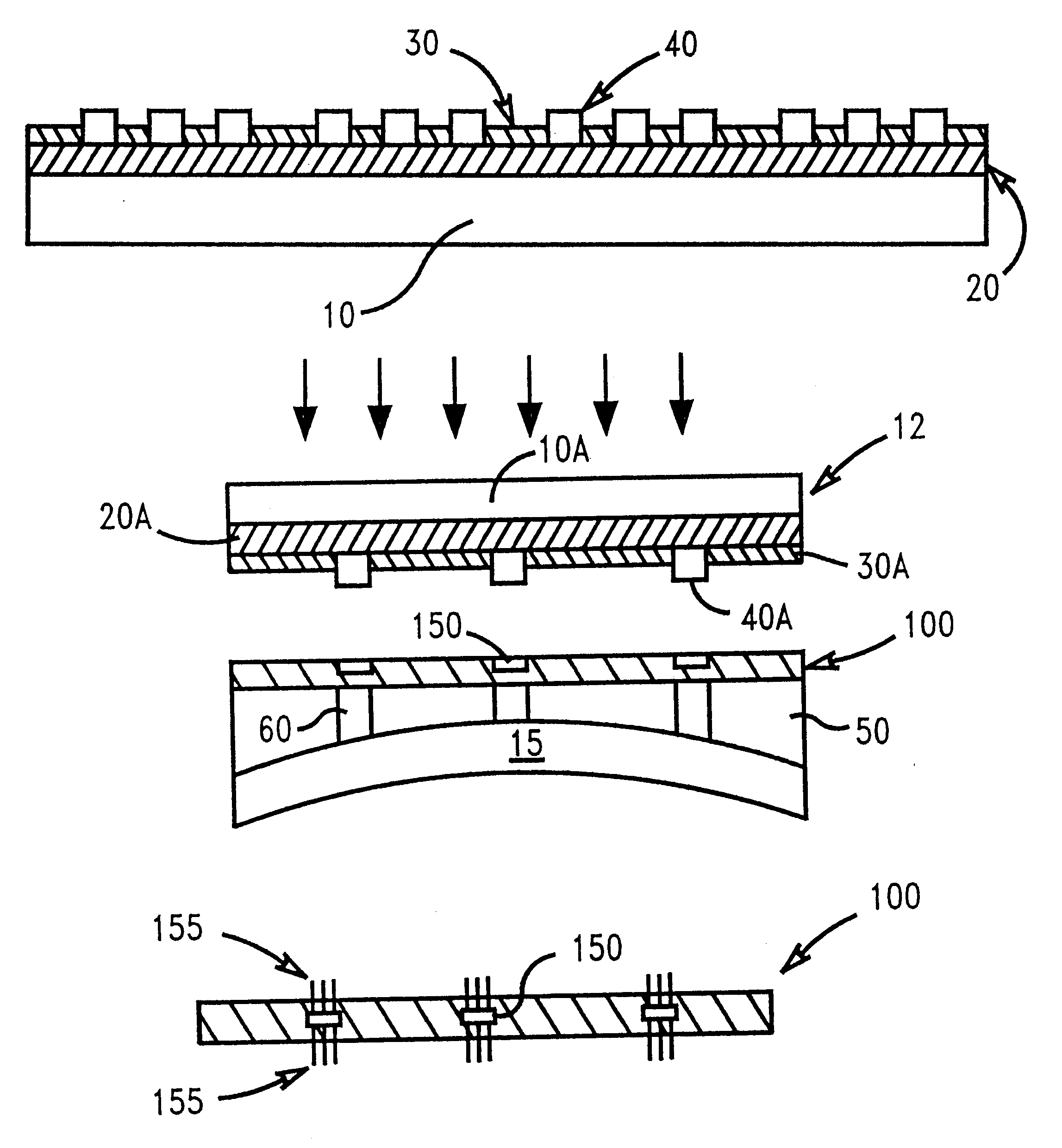
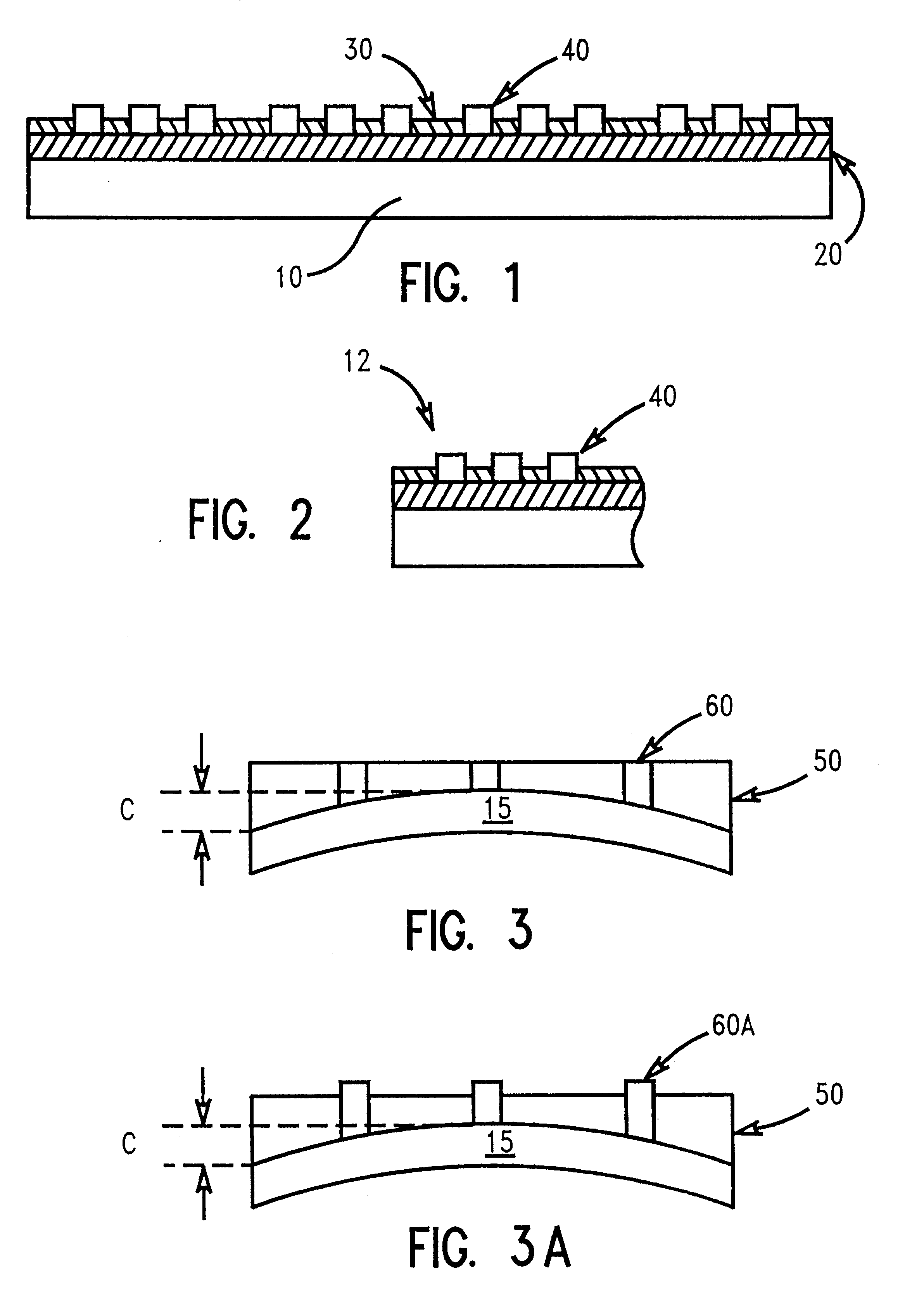
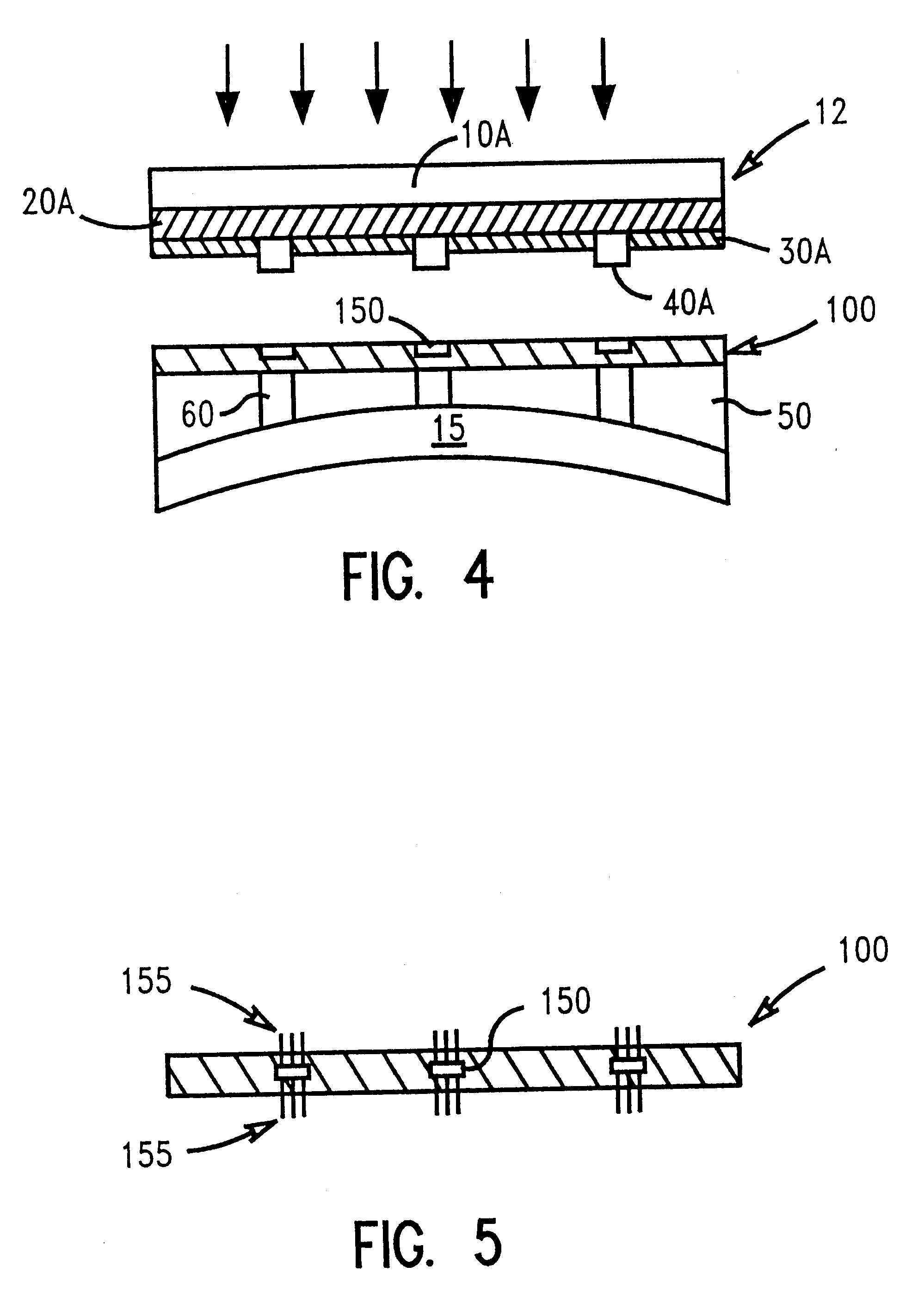
In describing the preferred embodiment of the present invention, reference will be made herein to FIGS. 1-5 of the drawings in which like numerals refer to like features of the invention. Features of the invention are not necessarily shown to scale in the drawings.

The present invention discloses a novel interconnect methodology using a substantially lead-free stud that provides an essentially planar surface for chip to substrate interconnection. The present invention reduces the difficulties encountered when joining a chip to a substrate having deformities on the substrate surface which cause the traditional solder interconnects to flow away from a solder pad that it is not in contact with. Additionally, the use of an interconnect technology which does not utilize lead based solder is of significant environmental benefit.

In preparing a chip and substrate for interconnection in accordance with the present invention, an array of protruding lead-free metal studs are formed on the sili...


PUM


Abstract

A method of interconnecting electronic components by using a plurality of conductive studs on a surface of a first electronic component and a plurality of corresponding conductive vias on the surface of a second electronic component. Camber on the surface of electronic components may be overcome by coating the surface with a dielectric, planarizing the dielectric, and forming conductive vias corresponding to the contact pads thereon. The conductive studs are substantially lead-free and preferably comprise of copper.

Description

Aspects of the present invention are related to subject matter disclosed in co-pending applications entitled "Z-Axis Compressible Polymer With Fine Metal Matrix Suspension," Ser. No. 09 / 315,373 filed on even date herewith and assigned to the assignee of the present invention, the subject matter of which is hereby incorporated by reference.1. Field of the InventionThis invention relates to electronic components which utilize a substantially lead-free interconnect process when forming an electronic module.2. Description of Related ArtAs the circuit density increases on integrated circuit devices such as silicon microprocessors, there is a need for high density interconnection between such a device and a chip carrier to which these devices are typically attached. Traditional methods of joining using solder ball arrays may become difficult with such dense circuitry.Typically, solder ball arrays require fluxes when joining lead based solders. With connection densities reaching about 150 ...

Claims


Application Information

Patent Timeline
IPC IPC(8): H01L21/60H01L21/02H01L23/498H01L23/48H05K3/32
CPCH01L23/49827H05K3/325H01L24/81H01L2924/014H01L2224/13147H01L2224/81801H01L2924/01029H01L2924/01079H01L2924/01082H01L2924/14H01L2924/3511H05K2201/0367H05K2201/09481H05K2201/10378H01L2924/01005H01L2924/01006H01L2924/01024H01L2924/01033H01L2924/01047H01L2924/12042H01L2924/15787H01L2924/00
Inventor BROFMAN, PETER J.RAY, SUDIPTA K.STALTER, KATHLEEN A.
Owner IBM CORP
Why Eureka
Try Eureka