Wafer probe card

a probe card and probe technology, applied in the direction of individual semiconductor device testing, fault location by increasing destruction at fault, instruments, etc., can solve the problems of defects identified in these parts, devices that likely would fail before the end of their specified life, and defects found at this stage of testing

Inactive Publication Date: 2001-07-24
SCS HIGHTECH +1
View PDF4 Cites 72 Cited by
  • Summary
  • Abstract
  • Description
  • Claims
  • Application Information

AI Technical Summary

Problems solved by technology

The defects found at this stage of testing typically originated during device fabrication.
Those devices lost during burn-in are devices that likely would fail before the end of their specified life during normal operation.
Defects are identified in these parts because the failure modes of the parts are accelerated by the burn-in process.
High-density memory integrated circuits, e.g. 64 megabit or larger memory chips, require even longer test times than prior generation memories, since more time is needed to test these larger memory chips due to the longer execution test pattern.
This more significant level of testing required by higher density memories can be costly and time-consuming.
Conventional wafer probe technology may only test a single die at a time, or at most, up to 32 die simultaneously, and simultaneous testing of a greater number of die is constrained, in part, by the physical limitation of probe tip design.
Conventional wafer probing systems

Method used


Image

  • Wafer probe card
  • Wafer probe card
  • Wafer probe card

Examples


Embodiment Construction

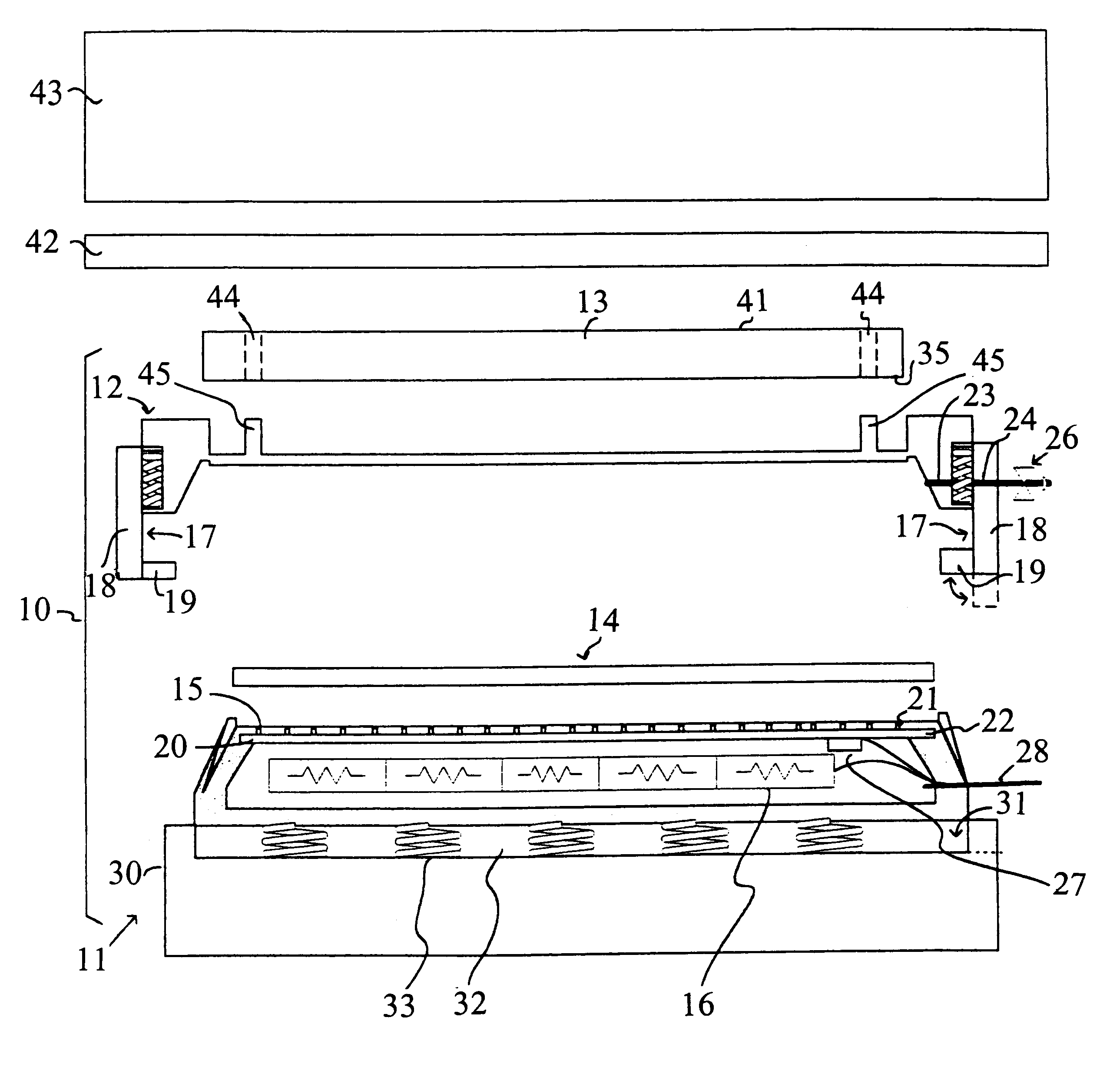
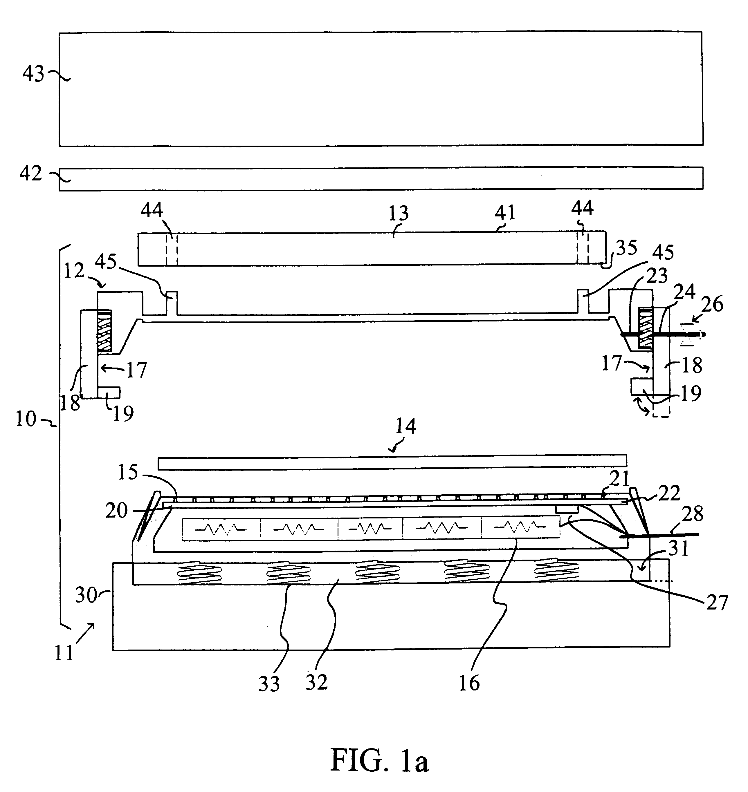
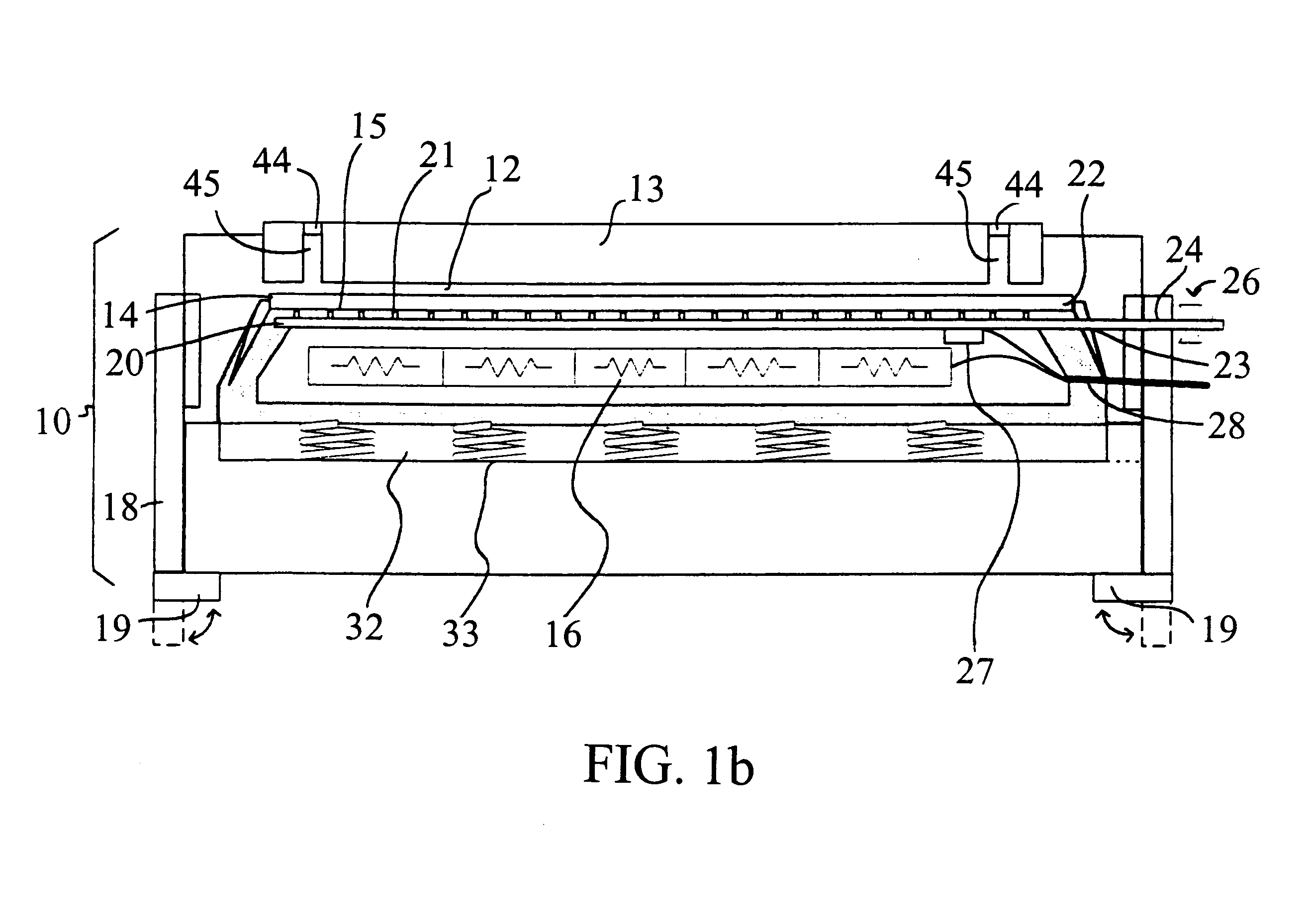
The present invention relates to a probe card with a short probe length to enable high temperature, high speed testing of high density devices while reducing the impedance mismatching problems typically associated with such testing. The invention may also relate to a probing and heating apparatus that uses the probe card to enable substrate level testing at elevated temperatures and methods for using the apparatus to test and burn-in devices at the substrate, e.g. wafer, level.

A probe card for electrically interfacing a plurality of devices on a substrate to be tested to a testing unit includes a plurality of probe tips disposed on a surface of the probe card facing the substrate and arranged in a manner corresponding to a plurality of contact pads on the devices of the substrate. The probe card also includes a plurality of signal contacts for conducting signals to and from the testing unit, each signal contact electrically connected to a probe tip. Use of preferred embodiments of t...


PUM


Abstract

An apparatus to heat and test a semiconductor wafer includes a probe card and tests a plurality of die simultaneously at the wafer level. In the present invention, the apparatus heats the wafer to sufficient temperatures to perform burn-in and a speed test. A method of testing the semiconductor allows certain die to be repaired that would otherwise be scrapped in a conventional process where bun-in and other tests are performed on packaged die. The method also eliminates steps associated with handling individually packaged parts, reduces burn-in space and consolidates certain test steps.

Description

1. Field of the InventionThe present invention relates generally to semiconductor testing devices and to testing and / or burn-in methods for semiconductor devices, and particularly to the testing of high density integrated circuits such as DRAMs, SRAMs and embedded devices including "system on a chip" and graphic accelerators with embedded DRAM.2. Description of the Related Art Integrated circuit devices, including DRAM and SRAM memory devices, are typically tested several times at the wafer level and again after dicing and packaging to ensure device quality and reliability. In a conventional testing process, individual devices on the wafer are tested to distinguish good devices from defective ones. The defects found at this stage of testing typically originated during device fabrication. If redundant circuits are present on the devices, a test / sort process is performed to detect reparable devices, which are typically laser repaired to activate the redundant circuitry. The good devic...

Claims


Application Information

Patent Timeline
IPC IPC(8): G01R31/28G01R1/073
CPCG01R31/2863G01R1/07314G01R31/2862G01R31/2831
Inventor HSU, HOWARD
Owner SCS HIGHTECH
Why Eureka
Try Eureka