Eureka AIR delivers breakthrough ideas for toughest innovation challenges, trusted by R&D personnel around the world.

Tungsten interconnect method

Inactive Publication Date: 2001-08-14
GLOBALFOUNDRIES INC
View PDF16 Cites 11 Cited by
  • Summary
  • Abstract
  • Description
  • Claims
  • Application Information

AI Technical Summary

Problems solved by technology

Despite the several advantages offered by tungsten as an interconnect material, the integration of tungsten into semiconductor processing involves a number of significant challenges.
Tungsten exhibits poor adhesion to oxide.
The difficulty with this approach is the potential for non-conformal tungsten deposition in the trench.
At relatively high silane flow rates, tungsten may deposit at a higher rate near the top of the trench than at the bottom, resulting in a bridge-over of the trench opening and the creation of a void in the tungsten interconnect.
Such voids may adversely impact the performance of the interconnect.
The incorporation of TiF.sub.x compounds into the adhesion layer may not only degrade the resistivity of the barrier layer, but also result in the ultimate delamination of the barrier glue layer from the underlying oxide layer.
This can produce not only undesirable device performance but also catastrophic device failure depending upon the extent of the delamination.
The problem of fluorine attack may be more pronounced in circumstances where the barrier film is deliberately fabricated with a small thickness or has thickness variations due to process control issues.
In addition, sometimes unavoidable process control variations in the etching of the interconnect trench may produce thin spots in the barrier film.
These thin spots represent areas that may be particularly susceptible to fluorine attack.

Method used


Image

  • Tungsten interconnect method
  • Tungsten interconnect method
  • Tungsten interconnect method

Examples


Embodiment Construction

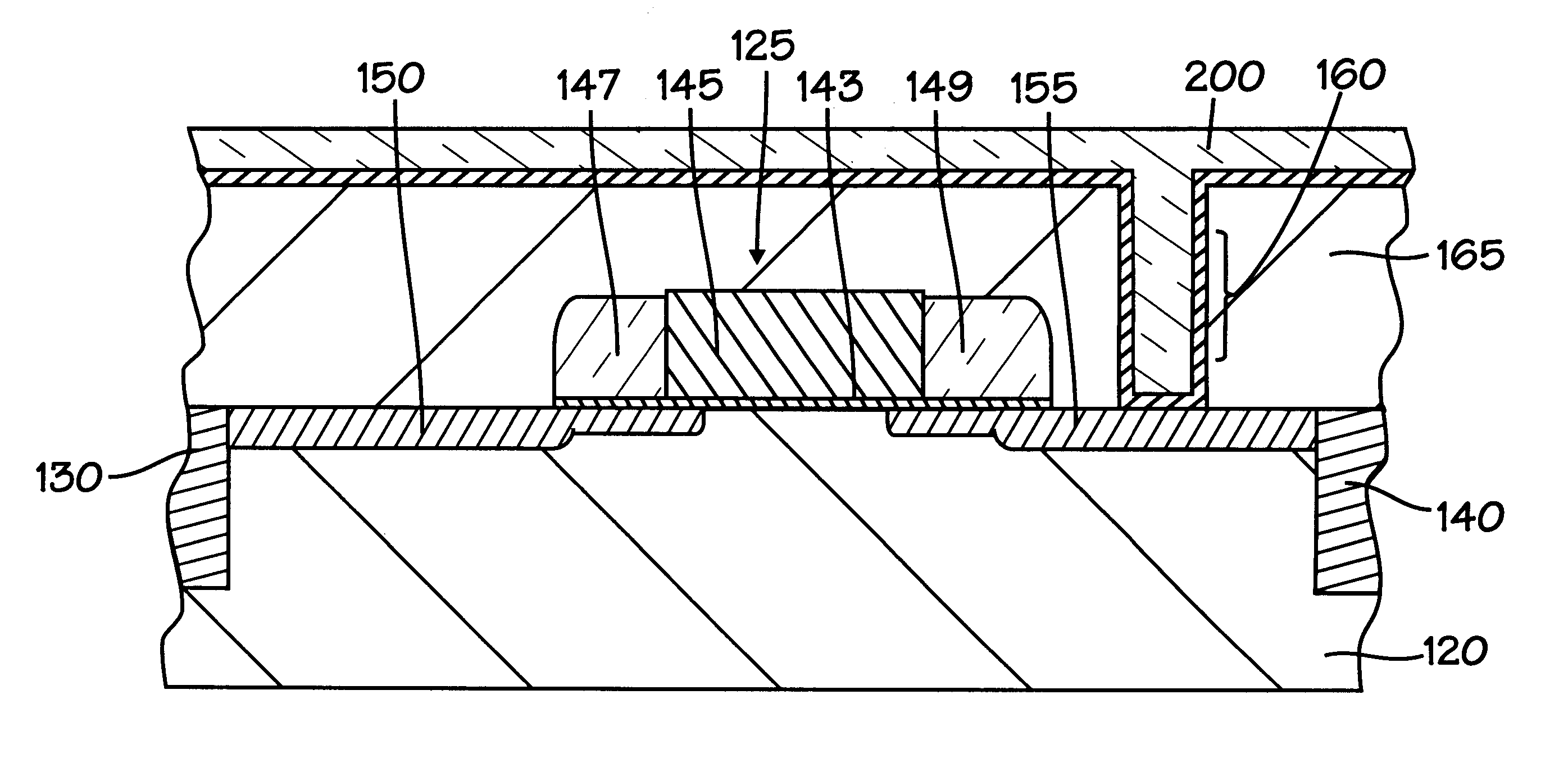
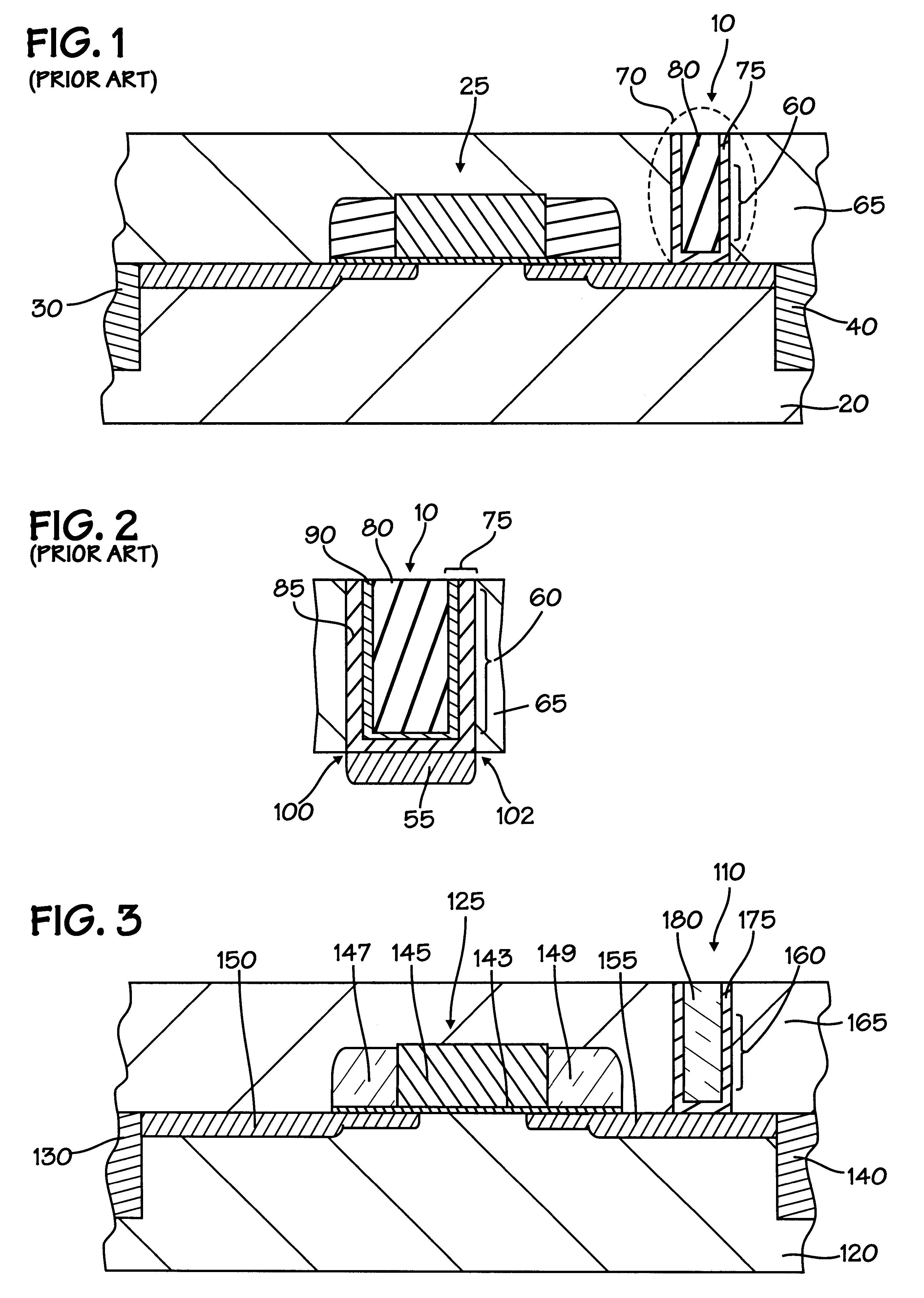
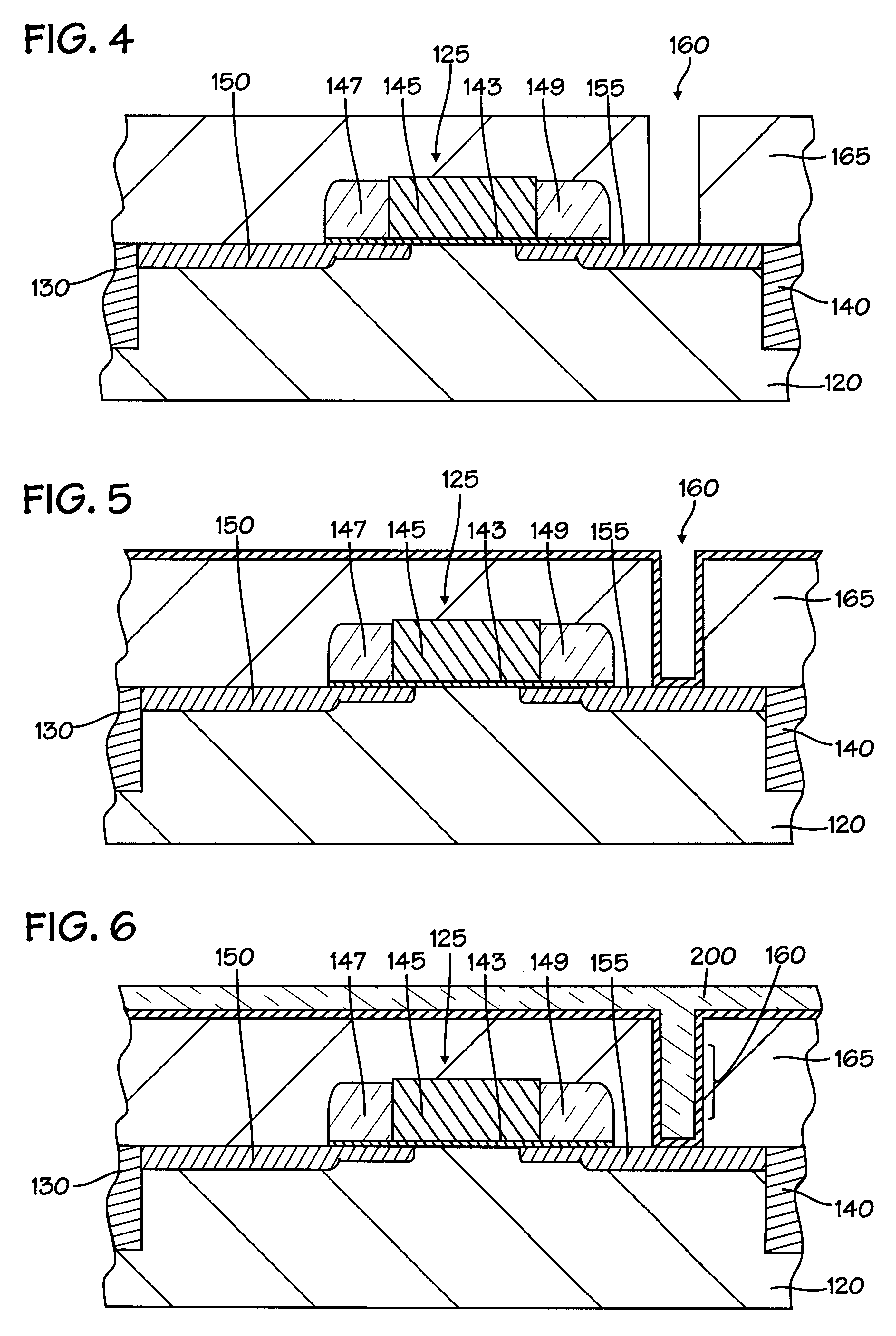
In the drawings described below, reference numerals are generally repeated where identical elements appear in more than one figure. FIG. 1 depicts a cross-sectional view of an exemplary conventional tungsten contact 10 fabricated on a semiconductor substrate 20. The contact 10 is depicted adjacent to an integrated circuit transistor 25 that is fabricated on the substrate 20 and electrically isolated laterally by isolation structures 30 and 40. The transistor 25 is depicted as a field effect transistor with a source 50 and a drain 55. The tungsten contact 10 is formed in a via 60 in an oxide interlevel dielectric layer 65, which is formed over the transistor 25.

The detailed structure of the tungsten contact 10 may be understood by referring now also to FIG. 2, which is a magnified view of the portion of FIG. I circumscribed by the dashed oval 70. The tungsten contact 10 consists of an adhesion layer 75 formed in the via 60 and a tungsten plug 80 formed on the adhesion layer 75. The a...


PUM


Abstract

A tungsten gate electrode and method of fabricating the same are provided. In one aspect, a method of fabricating a circuit device in an opening in an insulating film on a substrate is provided. The method includes depositing a film of amorphous silicon and amorphous tungsten in the opening, and thereafter depositing a film of polycrystalline tungsten on the film and annealing the substrate to react the amorphous silicon with the amorphous tungsten to form tungsten silicide on the insulating film and to increase the grain structure of the polycrystalline tungsten film. The tungsten silicide film and the polycrystalline tungsten film may be planarized to the insulating film. The method enables the seamless fabrication of an adhesion layer and a tungsten conductor structure in a single chamber and without resort to titanium.

Description

1. Field of the InventionThis invention relates generally to semiconductor fabrication, and more particularly to a tungsten interconnect and methods of fabricating the same.2. Description of the Related ArtModern integrated circuits routinely contain millions of individual transistors and other electronic components. Most of the interconnections for the numerous individual transistors in a modern integrated circuit are provided via one or more metallization layers that serve as global interconnect levels. Each metallization layer is ordinarily deposited on the substrate of the integrated circuit as a single continuous layer that is thereafter patterned lithographically and etched to remove metal from areas where metal lines are not required.In addition to the one or more metallization layers, modern integrated circuits also incorporate numerous routing-restricted interconnect levels commonly known as local interconnects. Local interconnects are used for short metallization runs such...

Claims


Application Information

Patent Timeline
IPC IPC(8): H01L21/768H01L21/02H01L21/70H01L21/3205
CPCH01L21/32053H01L21/76877H01L21/76864H01L21/76843
Inventor HOSSAIN, TIMOTHY Z.GHATAK-ROY, AMIYA R.EVANS, ALLEN
Owner GLOBALFOUNDRIES INC
Why Eureka
Eureka Blog
Learn More