Eureka AIR delivers breakthrough ideas for toughest innovation challenges, trusted by R&D personnel around the world.

Methods for growing low-resistivity tungsten for high aspect ratio and small features

a technology of low-resistance tungsten and nucleation layers, which is applied in the direction of coatings, chemical vapor deposition coatings, metallic material coating processes, etc., can solve the problems of limited ability to provide nucleation layers for the deposition of low-resistance tungsten in small features with high aspect ratios, and cannot be produced easily and reliably. , to achieve the effect of low-resistan

Inactive Publication Date: 2011-09-15
NOVELLUS SYSTEMS
View PDF98 Cites 43 Cited by
  • Summary
  • Abstract
  • Description
  • Claims
  • Application Information

AI Technical Summary

Problems solved by technology

The bulk layer is generally deposited more rapidly than the nucleation layer, but cannot be produced easily and reliably without first forming the nucleation layer.
Although CVD and other methods have been able to deposit nucleation layers, their ability to provide nucleation layers for the deposition of low resistivity tungsten in smaller features with high aspect ratios is limited.

Method used


Image

  • Methods for growing low-resistivity tungsten for high aspect ratio and small features
  • Methods for growing low-resistivity tungsten for high aspect ratio and small features
  • Methods for growing low-resistivity tungsten for high aspect ratio and small features

Examples


example 1

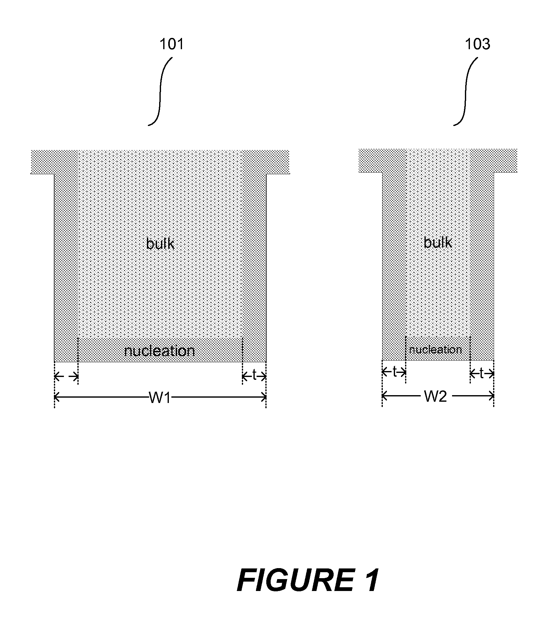
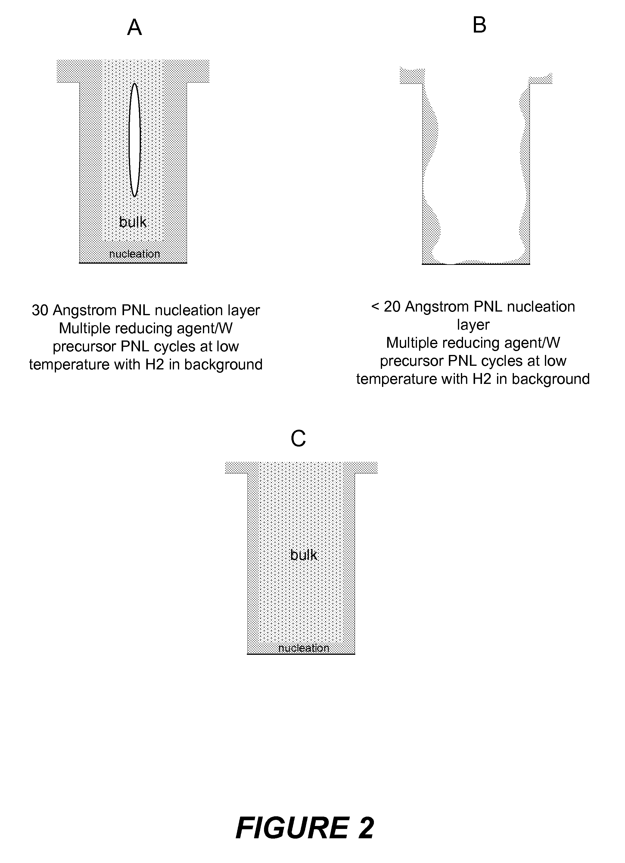
[0037]A W nucleation layer was formed in a feature having an AR of 30:1 and a 0.15 μm opening the following pulsed nucleation layer process:[0038]5 Torr, 300 C, B2H6 dose (7.5 sec.), 10 sec. purge, WF6 dose (10 sec)[0039]A W bulk layer was then formed using a CVD process (H2-WF6) at 80 Ton and 395 C.

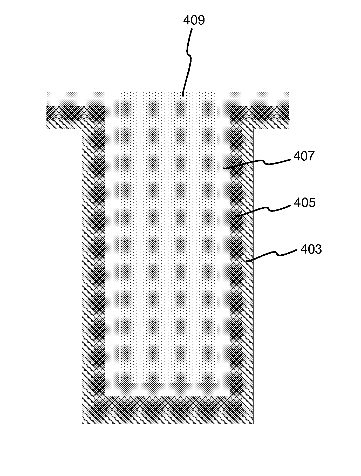
[0040]The thickness of the nucleation layer was about 80 Angstroms. Total thickness was 2000 Angstroms. Resisitivity was of the film as measured on a blanket wafer was 11 μΩ-cm. Step coverage was greater than 90%.

example 2

[0041]A W nucleation layer was formed in a feature having a 10:1 AR and a 0.075 μm opening using the following pulsed nucleation layer process:[0042]40 Ton, 300 C, B2H6 dose (1 sec.), 3 sec. purge, WF6 dose (0.5 sec), 3 sec purge (5 cycles)[0043]W bulk layer was then formed using a CVD process (H2-WF6) at 40 Ton and 395 C.

[0044]The thickness of the nucleation layer was about 20 Angstroms. Total thickness was 2000 Angstroms. Resisitivity was of the film as measured on a blanket wafer was 11 μΩ-cm. Step coverage was greater than 90%.

Apparatus

[0045]The methods of the invention may be carried out in various types of deposition apparatus available from various vendors. Examples of suitable apparatus include a Novellus Concept-1 Altus, a Concept 2 Altus, a Concept-2 ALTUS-S, a Concept 3 Altus deposition system, or any of a variety of other commercially available CVD tools. In some cases, the process can be performed on multiple deposition stations sequentially. See, e.g., U.S. Pat. No. 6,...


PUM

PropertyMeasurementUnit
aspect ratioaaaaaaaaaa
currentaaaaaaaaaa

Abstract

The present invention addresses this need by providing methods for depositing low resistivity tungsten films in small features and features having high aspect ratios. The methods involve depositing very thin tungsten nucleation layers by pulsed nucleation layer (PNL) processes and then using chemical vapor deposition (CVD) to deposit a tungsten layer to fill the feature. Depositing the tungsten nucleation layer involves exposing the substrate to alternating pulses of a boron-containing reducing agent and a tungsten-containing precursor without using any hydrogen gas, e.g., as a carrier or background gas. Using this process, a conformal tungsten nucleation layer can be deposited to a thickness as small as about 10 Angstroms. The feature may then be wholly or partially filled with tungsten by a hydrogen reduction chemical vapor deposition process. Resistivities of about 14 μΩ-cm for a 500 Angstrom film may be obtained.

Description

CROSS-REFERENCE TO RELATED APPLICATIONS[0001]This application is a continuation of and claims priority to U.S. application Ser. No. 12 / 030,645, filed Feb. 13, 2008, titled “Methods for Growing Low-Resistivity Tungsten for High Aspect Ratio and Small Features,” which claims the benefit of U.S. Provisional Patent Application No. 60 / 904,015, filed Feb. 27, 2007, and is also a continuation-in-part of U.S. patent application Ser. No. 11 / 265,531 (now U.S. Pat. No. 7,589,017), filed Nov. 1, 2005, titled “Methods For Growing Low-Resistivity Tungsten Film,” which in turn is a continuation-in-part of U.S. patent application Ser. No. 10 / 815,560 (now U.S. Pat. No. 7,262,125), filed Mar. 31, 2004, titled “Method of Forming Low-Resistivity Tungsten Interconnects,” which in turn is a continuation-in-part of U.S. patent application Ser. No. 10 / 649,351 (now U.S. Pat. No. 7,141,494), filed on Aug. 26, 2003, titled “Method for Reducing Tungsten Film Roughness and Improved Step Coverage,” which is in t...

Claims


Application Information

Patent Timeline
Patent Type & Authority Applications(United States)
IPC IPC(8): H01L21/768
CPCC23C16/0281C23C16/045C23C16/14H01L21/76877H01L21/28556H01L21/28562H01L21/76876C23C16/45525
Inventor CHAN, LANA HIULUIASHTIANI, KAIHANCOLLINS, JOSHUA
Owner NOVELLUS SYSTEMS
Why Eureka
Eureka Blog
Learn More