

Method for forming tungsten film, film-forming apparatus, storage medium and semiconductor device
a technology of tungsten film and film-forming apparatus, which is applied in the direction of basic electric elements, chemical vapor deposition coatings, coatings, etc., can solve problems such as volcano formation or holes, and achieve the effect of preventing volcano formation, specific resistance of tungsten film, and improving adhesion of tungsten film to the base barrier layer
- Summary
- Abstract
- Description
- Claims
- Application Information
AI Technical Summary
Benefits of technology
Problems solved by technology
Method used
Image

Examples
Embodiment Construction
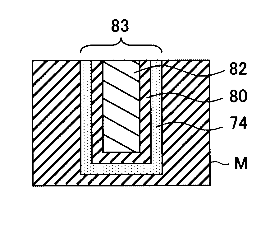
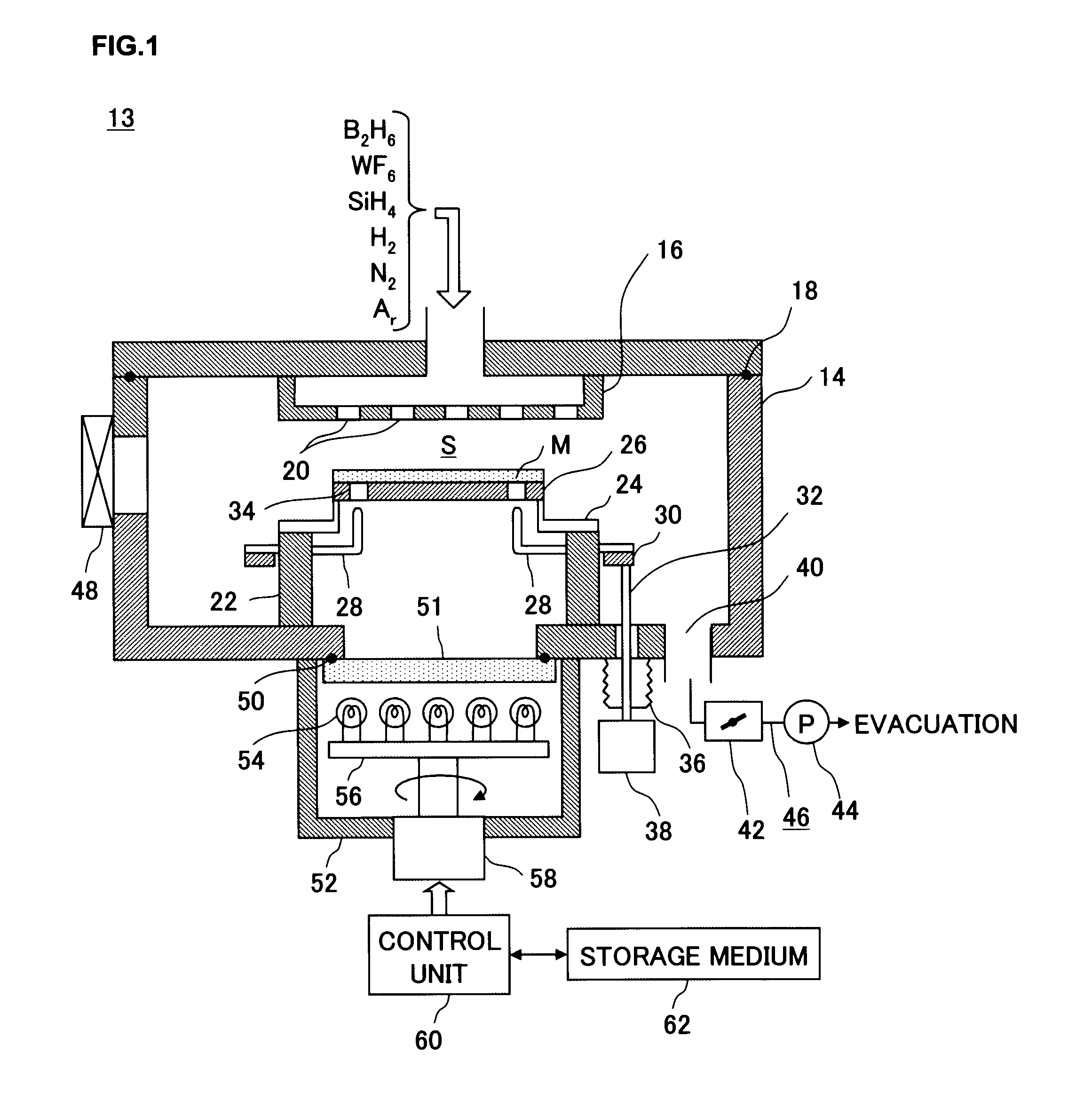
[0085]The following is a detailed explanation of the best mode for carrying out the present invention given in reference to the attached drawings. It is to be noted that in the description and the drawings, the same reference numerals are assigned to components having substantially identical functions and structural features to preclude the necessity for a repeated explanation thereof.
(Structural Example for the Film Forming Apparatus)
[0086]FIG. 1 shows the structure of a film forming apparatus that may adopt the tungsten film formation method achieved in an embodiment of the present invention in a sectional view. As shown in FIG. 1, the film forming apparatus 13 includes an aluminum processing container 14 having, for instance, a substantially cylindrical section. A showerhead unit 16 functioning as a gas supply means for delivering various types of film formation gases, an inert gas and the like, to be used as processing gases, into the processing container 14 at controlled flow r...
PUM
| Property | Measurement | Unit |
|---|---|---|
| thickness | aaaaa | aaaaa |
| thickness | aaaaa | aaaaa |
| temperature | aaaaa | aaaaa |
Abstract
Description
Claims
Application Information