Connector for module

Inactive Publication Date: 2001-08-21
JST MFG CO LTD
View PDF4 Cites 52 Cited by
  • Summary
  • Abstract
  • Description
  • Claims
  • Application Information

AI Technical Summary

Problems solved by technology

This thermal load may cause deformation of the arms of the connector, which in turn may result in loss of the engaging function of the engaging members.
Outward elastic deformation of the top ends of the arms by fingers may cause plastic deformation of the arms.
The loss of the engaging function and the deformation may

Method used


Image

  • Connector for module
  • Connector for module
  • Connector for module

Examples


first embodiment

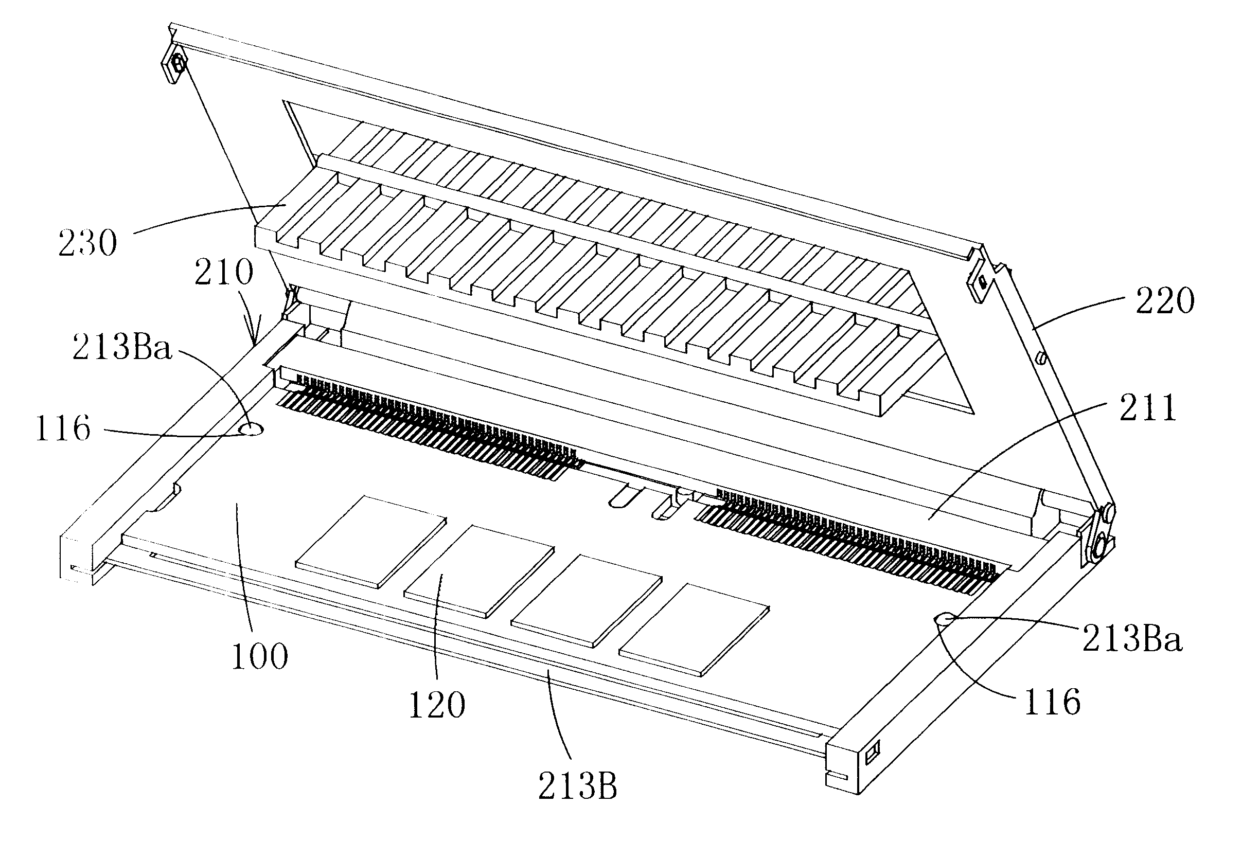
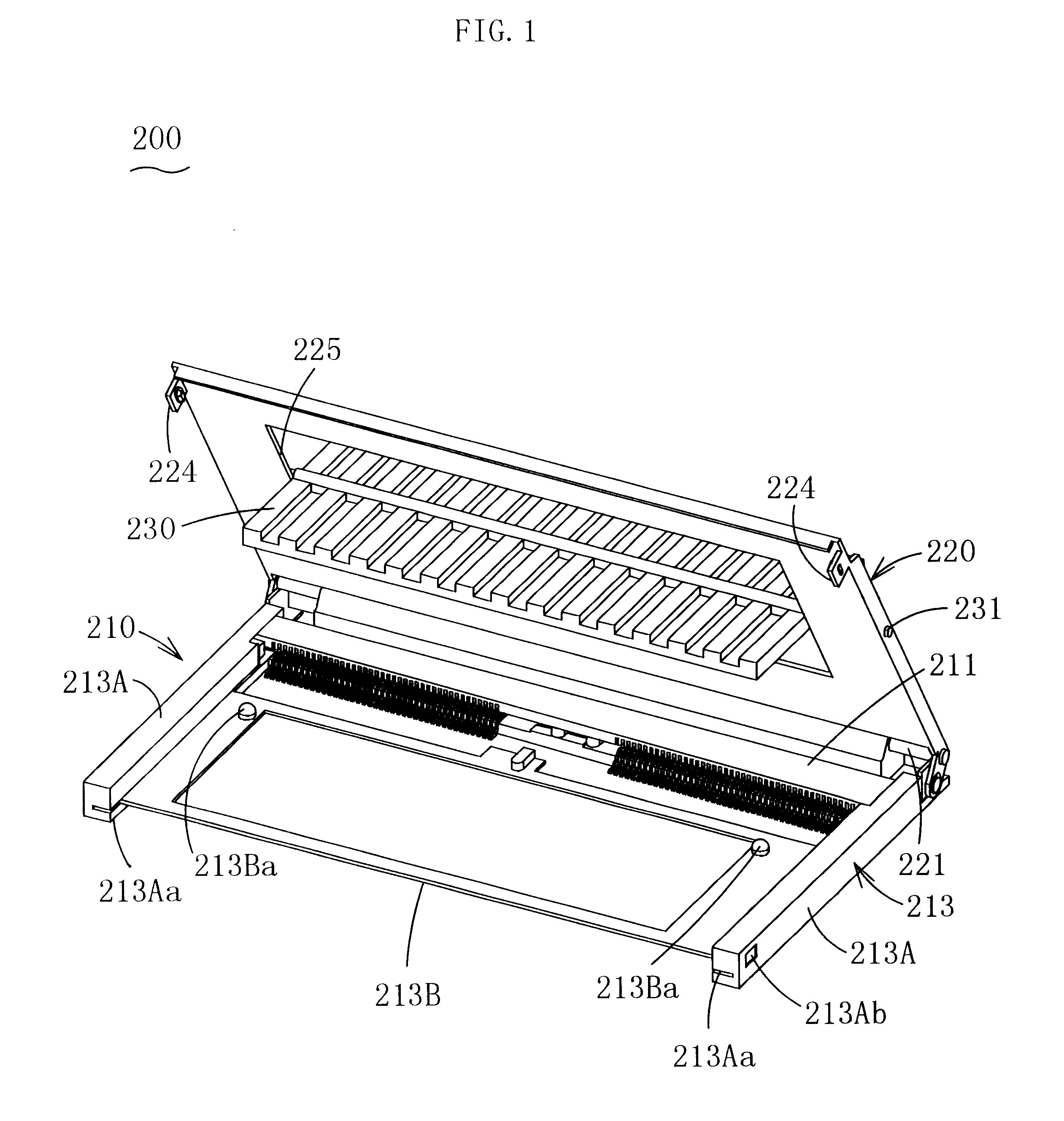
the connector for module is mounted on a printed circuit board 300 by, for example, soldering the solder tails of the contacts 212a, 212b onto the printed circuit board 300 and, when necessary, fixing the bases 213A of the supporting part 213 on the printed circuit board 300. When a module 100 is to be fitted into the connector 200, the module 100 is placed on the slider 213B when the rear end of the metal cover 220 is up, then the rear end of the metal cover 220 is lowered. As a result, the slider 213B will move forward, and the front side 111 of the module 100 will enter into the groove 211a of the receiving part 211 and the front side 111 will be inserted into the space between the contacts 212a, 212b and the conductive pads 130 will contact the contacts 212a, 212b. When the metallic cover 220 is put over the module 100 and engaged to the connector body 210, the module 100 will be sandwiched between the supporting part 213 and the metallic cover 220 and kept in the connection pos...

second embodiment

With the arrangement of the second embodiment, as the contacting surface of the heat sink 230 is reliably brought to face-to-face contact with the surfaces of semiconductor chips 120, the heat of the semiconductor chips 120 is efficiently transferred to the heat sink 230. Hence the semiconductor chips 120 are cooled well and their operation is maintained stably. Moreover, as the heat sink 230 is energized towards the module by the elastic members 240, any error in the clearance between the heat sink 230 and the semiconductor chips 120 will be absorbed, and the contacting face of the heat sink 230 will contact the surface of the semiconductor chips 120 with an appropriate pressure. Hence the dispersion of the heat transfer performance from the semiconductor chips 120 to the heat sink 230 among the products can be reduced.

FIG. 19 and FIG. 20 show the third embodiment. This third embodiment differs from the second embodiment in that the location of the hinge axis 231 is at the front en...

fourth embodiment

With the arrangement of the fourth embodiment, as the contacting surface of the heat sink 230 is reliably brought to face-to-face contact with the surfaces of semiconductor chips 120, the heat of the semiconductor chips 120 is efficiently transferred to the heat sink 230. Hence the semiconductor chips 120 are cooled well and their operation is maintained stably. In this case, as the angle of fitting the heat sink 230 to the metallic cover 220 is variable in all directions, the ratio of success in the above-mentioned face-to-face touching is improved. Hence cooling of the semiconductor chips 120 is promoted further and their operation is maintained more stably. Moreover, as the heat sink 230 is energized towards the module by this supporting structure, any error in the clearance between the heat sink 230 and the semiconductor chips 120 will be absorbed, and the contacting face of the heat sink 230 will contact the surface of the semiconductor chips 120 with an appropriate pressure. H...


PUM


Abstract

A connector for module that connects a module to a printed circuit board in a position wherein the board plane of the module is approximately parallel to the printed circuit board. This connector comprises a connector body having a receiving part that extends along the front side of the module being in the connection position, having a contact that are provided in the receiving part and contact the conductive pad while allowing the pad to shift in the direction of insertion/withdrawal, and having a supporting part that extends rearward from the receiving part to carry the module being in the connection position and limits shifting of the module in the front-rear direction and the left-right direction, a metallic cover that is put over and is engaged to the connector body to sandwich the module between itself and the supporting part and keep the module in the connection position, having a window for exposing semiconductor chip of the module being in the connection position, and a heat sink that is arranged to contact the semiconductor chip in the windows and is connected to the metallic cover by a supporting structure that enables variation of the angle of fitting.This connector prevents defective connection or the like of the module due to thermal load, etc., reduces the effects of electromagnetic waves, etc. on the connector by its shielding function to maintain the operation of circuits stable, and cools the semiconductor chip to maintain their operation stable.

Description

1. Field of the InventionThe present invention belongs to a technical field of connector for module (hereinafter it may be simply referred to as connector) that is used for a module wherein semiconductor chips are mounted on a rectangular board and conductive pads are provided on a front side of the board (hereinafter simply referred to as module). In particular, the present invention relates to countermeasures against heat, electromagnetic waves, etc. to which a connector for module is exposed.2. Related ArtModules of this kind include those in which semiconductor chips such as semiconductor memories are mounted. A module connector is used extensively, which connects a module of this kind to a printed circuit board such as a mother board in a position wherein the board surface of the module is approximately parallel to the printed circuit board. This connector has an approximately U-shaped form to correspond to the front side, left side and right side of the module, respectively. A...

Claims


Application Information

Patent Timeline
IPC IPC(8): H01R12/00H01R12/16H05K7/14H01R24/00G06K19/077H01R12/72H01R12/88H01R13/514
CPCH05K7/1431H01R12/88H01R12/721H01R13/514
Inventor YASUFUKU, KAORIHOSAKA, TAI JIMIYAZAWA, MASAAKI
Owner JST MFG CO LTD
Why Eureka
Try Eureka