Method for fabricating ferroelectric memory

Inactive Publication Date: 2001-09-18
LG ELECTRONICS INC
View PDF2 Cites 38 Cited by
  • Summary
  • Abstract
  • Description
  • Claims
  • Application Information

AI Technical Summary

Problems solved by technology

However, the related art method for fabricating the SWL ferroelectric memory has the following problem.
The alignment allowance required between the wordlin

Method used


Image

  • Method for fabricating ferroelectric memory
  • Method for fabricating ferroelectric memory
  • Method for fabricating ferroelectric memory

Examples


Embodiment Construction

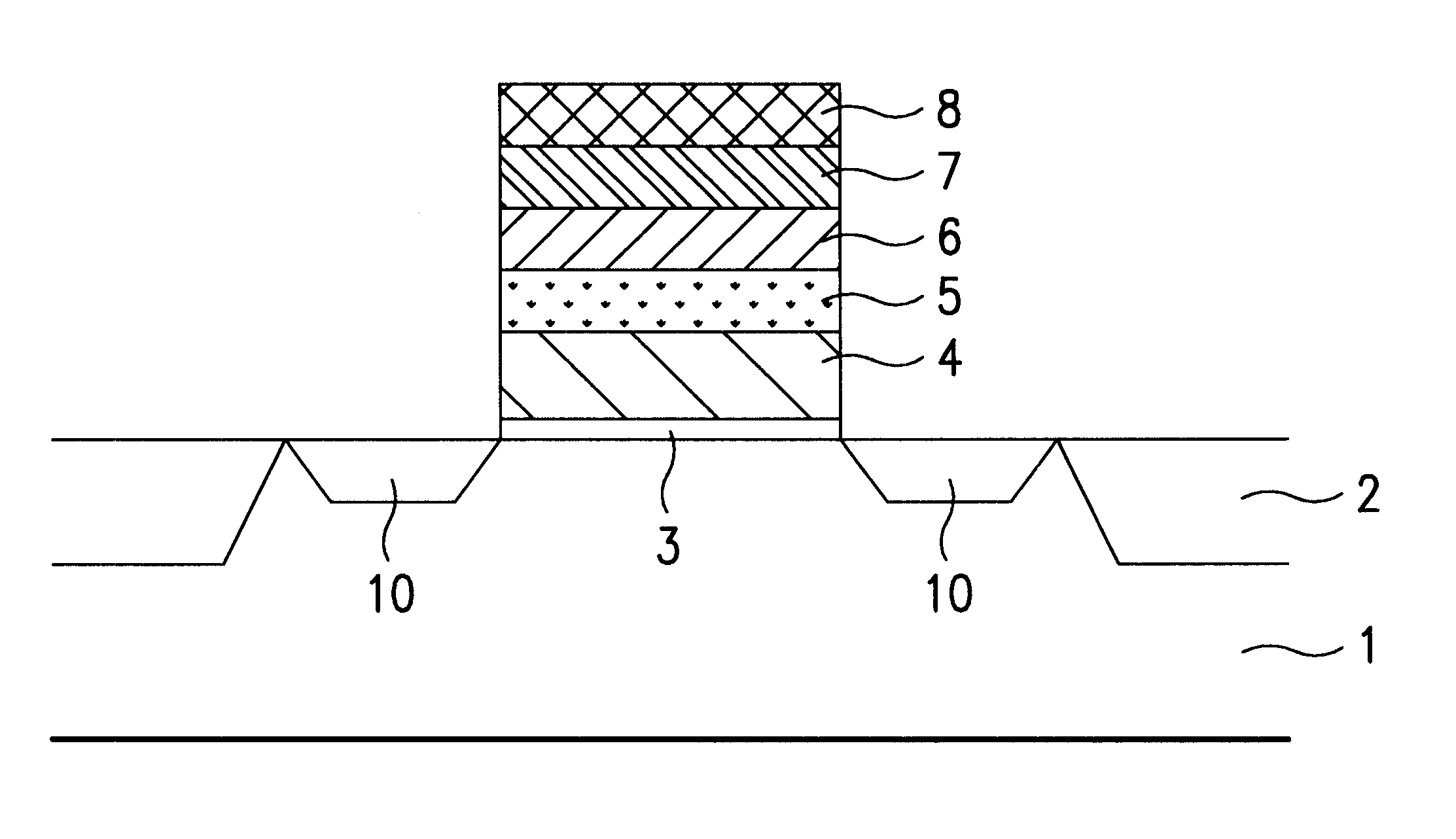
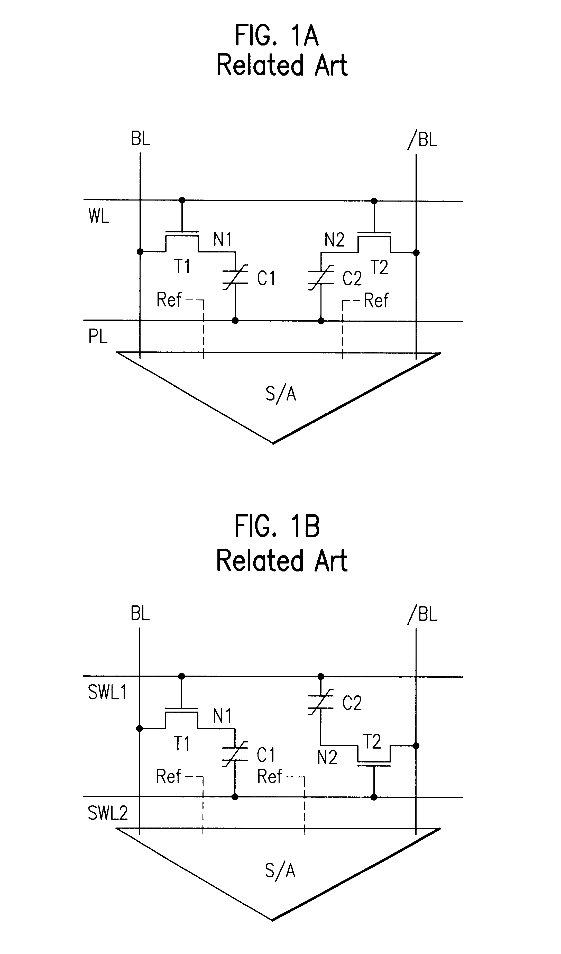
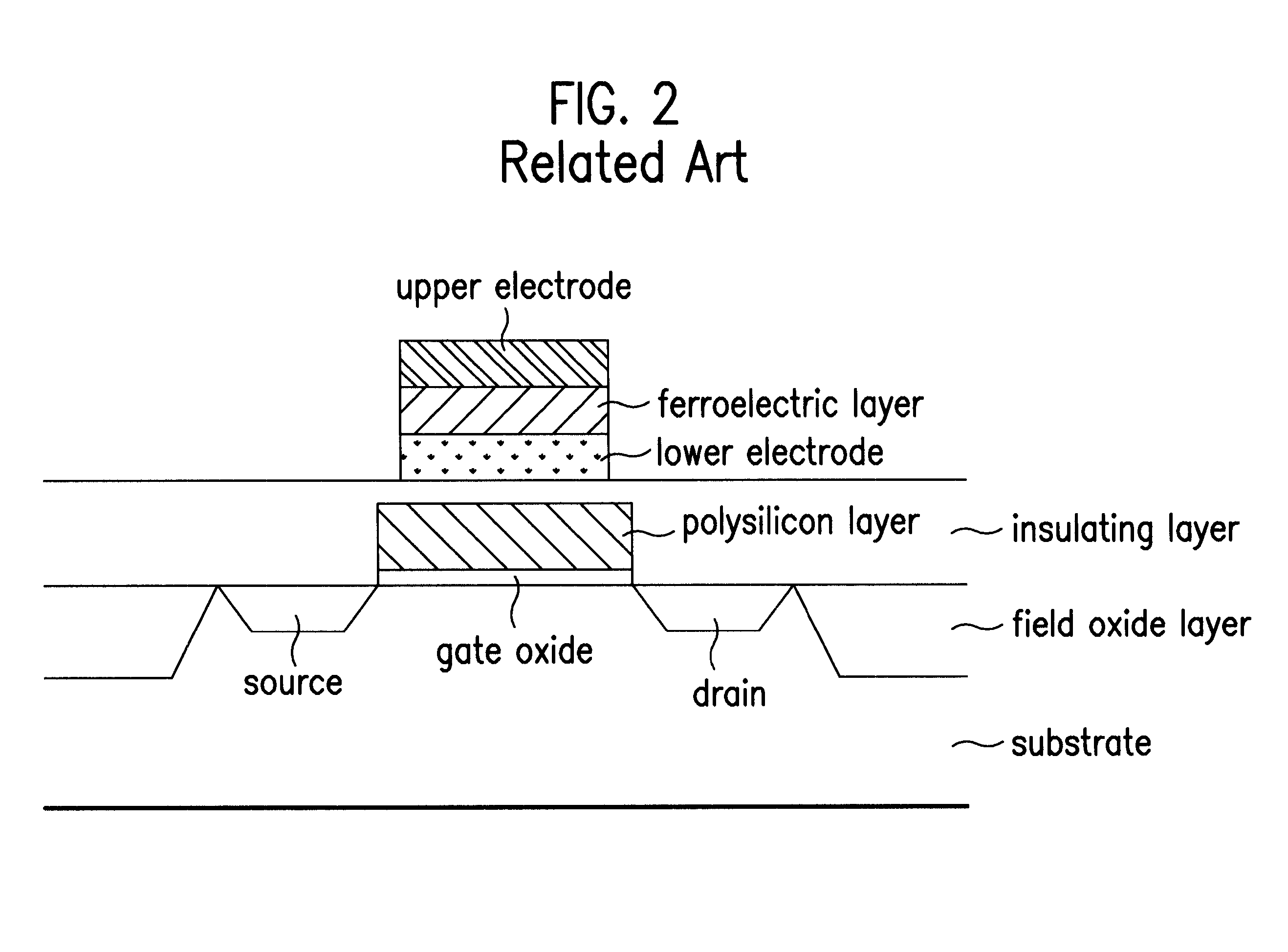
Reference will now be made in detail to the preferred embodiments of the present invention, examples of which are illustrated in the accompanying drawings. The present invention suggests a new method for supplementing the related art method for fabricating an SWL, ferroelectric memory, in which the lack of alignment allowance between the wordline and the SWL ferroelectric memory impedes fabrication of a memory with a high device packing density and requires many fabrication steps. A core of the present invention lies on employment of an etch stop layer and a metal mask of a high etch selectivity for etching a ferroelectric layer and a polysilicon layer at a time. FIGS. 3A.about.3G illustrate sections showing the steps of a method for fabricating an SWL ferroelectric memory in accordance with a preferred embodiment of the present invention.

Referring to FIG. 3A, after field oxide(SiO.sub.2) 2 is formed in a substrate for isolation between cells, as shown in FIG. 3B, a gate oxide(SiO.s...


PUM


Abstract

Method for fabricating a nonvolatile ferroelectric memory, including the steps of (1) forming an insulating layer, a semiconductor layer, an etch stop layer, a lower electrode, a ferroelectric layer, and an upper electrode on a substrate in succession, (2) forming an etch mask pattern of a required form on the upper electrode, (3) using the etch mask pattern as a mask in subjecting the upper electrode, the ferroelectric layer, the lower electrode, the etch stop layer, the semiconductor layer, and the insulating layer to en bloc etching, to expose the substrate, and (4) removing the etch mask pattern, and forming source/drain regions in the exposed substrate, whereby providing a simple fabrication process and permitting to minimize an alignment allowance.

Description

1. Field of the InventionThe present invention relates to a method for fabricating a nonvolatile ferroelectric memory.2. Background of the Related ArtFeRAM(Ferroelectric Random Access Memory) of a ferroelectric film has been widely studied as a memory which can replace nonvolatile memories, such as current flash memory, because, in general, the FeRAM not only has advantages of a fast writing speed, a low voltage driving, and a low power consumption, but also has a nonvolatile characteristic. In the current ferroelectric memories, there are ones with pairs of transistor and capacitor(1 transistor / 1 capacitor type, 2 transistor / 2 capacitor type), and ones with the ferroelectric film on a gate to form one transistor(1 transistor type). Researches for the ferroelectric memory is mostly focused on the 1 transistor / 1 capacitor type.In the meantime, recently a new type of SWL(Split Word Line) ferroelectric memory has been suggested, of which structure is as follows. FIG. 1A illustrates a c...

Claims


Application Information

Patent Timeline
IPC IPC(8): H01L29/66H01L21/28H01L21/02H01L29/78H01L27/108
CPCH01L21/28291H01L29/78391Y10S438/945H01L29/40111H10B12/00
Inventor NAM, HYO JIN
Owner LG ELECTRONICS INC
Why Eureka
Try Eureka