

Wide view angle LCD operable in IPS mode which uses a pixel electrode as a shield to prevent disturbances in the electric field of a display pixel portion of the LCD
a liquid crystal display device and wide view angle technology, applied in non-linear optics, identification means, instruments, etc., can solve problems such as display fluctuation problems
- Summary
- Abstract
- Description
- Claims
- Application Information
AI Technical Summary
Problems solved by technology
Method used
Image

Examples
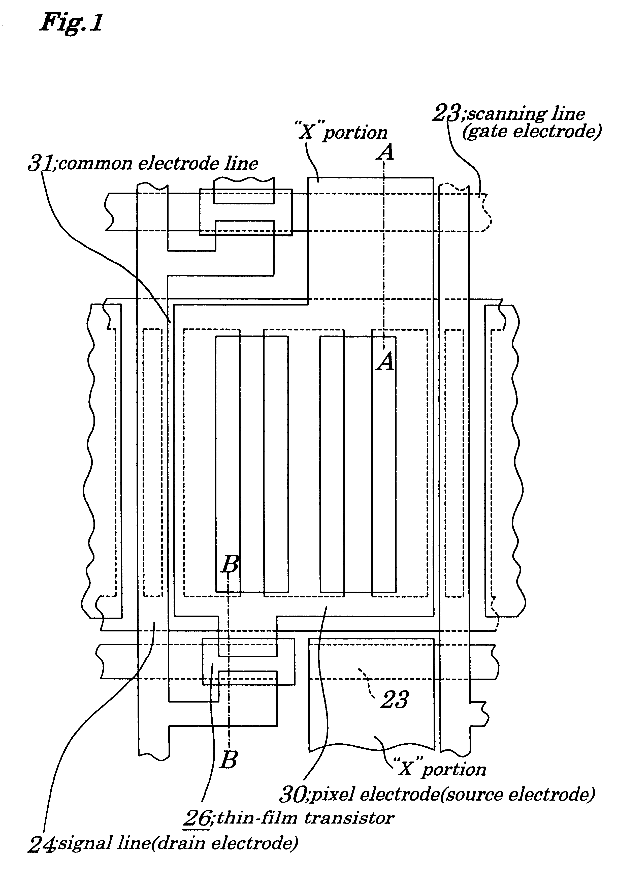
first embodiment
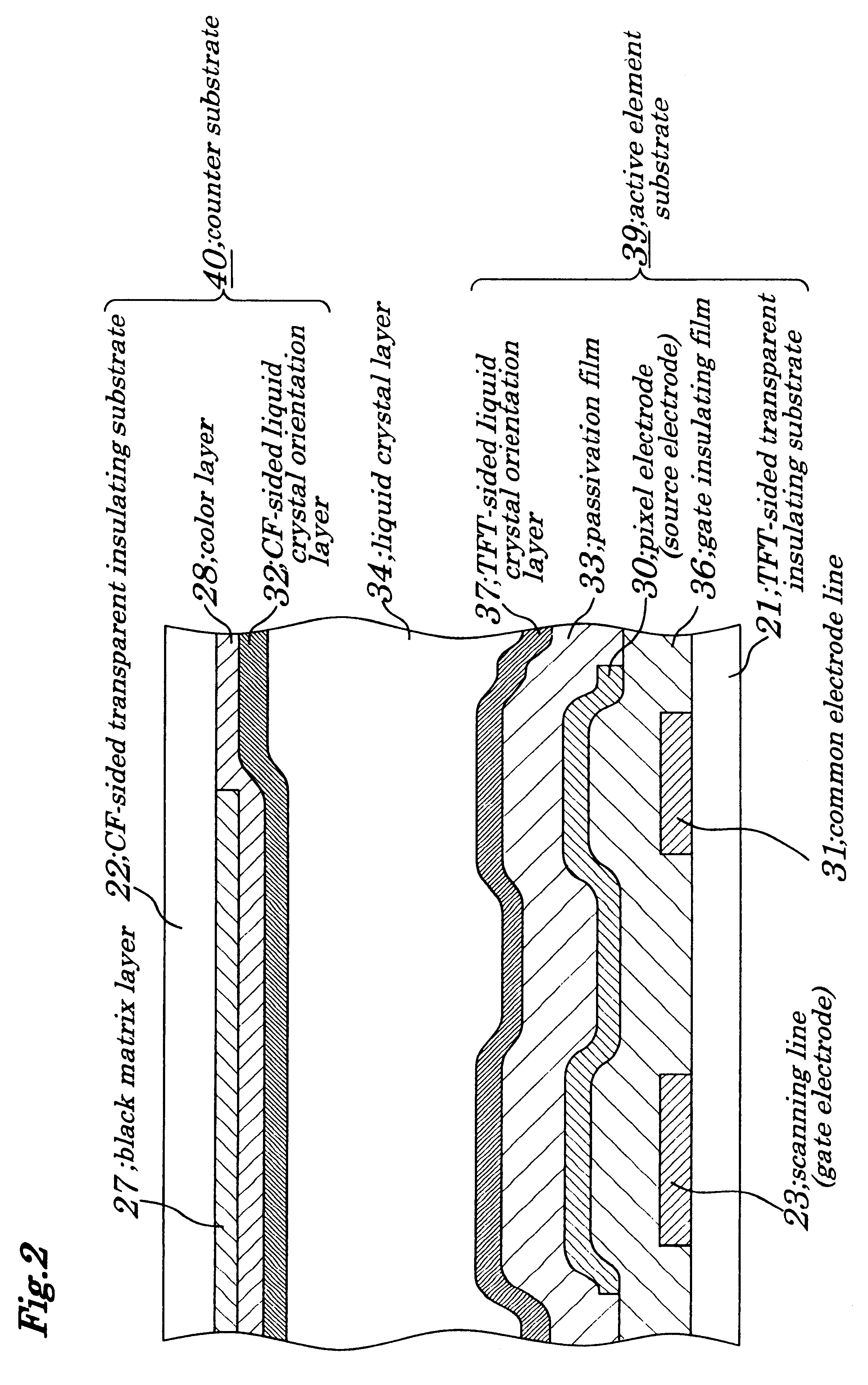
The wide view angle liquid crystal display device of this first embodiment is further arranged by a TFT-sided liquid crystal orientation film 37 formed on this passivation film 33.
In this embodiment, such an entire substrate arranged by the structural elements defined from the TFT-sided transparent insulating substrate 21 up to the TFT-sided liquid crystal orientation film 37 will now be defined as an "active element substrate" 39.
The wide view angle liquid crystal display device according to the first embodiment is additionally provided with a liquid crystal layer 34 by which liquid crystal molecules are sealed. This liquid crystal layer 34 is arranged in such a manner that while both the CF-sided liquid crystal orientation film 32 and the TFT-sided liquid crystal orientation film 37 are juxtaposed with respect to this liquid crystal layer 34, the liquid crystal layer 34 is sandwiched by the active element substrate 39 and the counter substrate 40.
It should also be understood that ...
second embodiment
Next, a description will be made of a second embodiment according to the present invention.
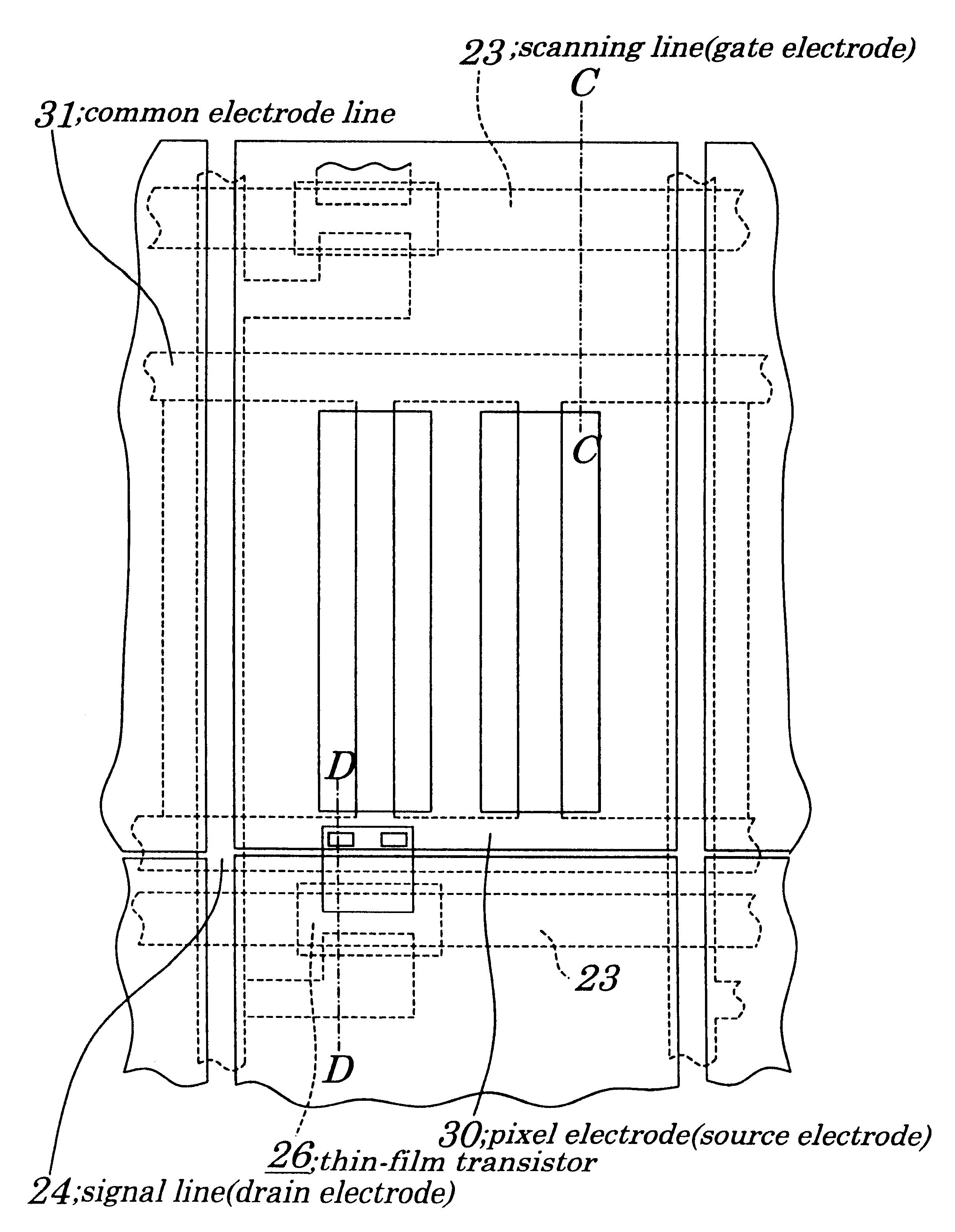
FIG. 4 is a plan view for schematically showing a structure of one pixel of a wide view angle liquid crystal display (LCD) device according to a second embodiment of the present invention. FIG. 5 is a sectional view for indicating the wide view angle LCD device according to the second embodiment, taken along a line C--C of FIG. 4. Also, FIG. 6 is a sectional view for representing the wide view angle LCD device according to the second embodiment, taken along a line D--D of FIG. 4.
Also, the wide view angle liquid crystal display device according to this second embodiment is so arranged as to be driven by an LCD drive method similar to that of the first embodiment.
As represented in FIG. 4 to FIG. 6, the wide view angle liquid crystal device of the second embodiment owns a different structure from that of the first embodiment. That is, in addition to the layers shown in the LCD device (see FIG. 3)...
PUM
 Abstract
Description
Claims
Application Information