Thin-film transistor and method of fabricating same

a thin film transistor and film technology, applied in the field of thin film transistors, can solve the problems of imposing restrictions on substrate materials, low cost of tfts manufacturing, and performance differences of crystalline silicon , to achieve the effect of improving performance and reducing manufacturing costs

Active Publication Date: 2008-12-16
PANASONIC CORP
View PDF13 Cites 0 Cited by
  • Summary
  • Abstract
  • Description
  • Claims
  • Application Information

AI Technical Summary

Benefits of technology

[0051]It should be noted that since the advantageous effects achieved by the present invention are attained by controlling the orientation direction of the π-conjugated organic semiconductor molecules used for the semiconductor layer to be in an appropriate direction with respect to the disposition of the source electrode and the drain electrode, the configuration of the TFT itself may be either of the configurations shown in FIG. 1 or 2; that is, the configuration is not limited to either one of the configurations. Accordingly, the following description discusses cases in which the configuration of the TFT 100 with the top gate design shown in FIG. 1C is employed as a representative example of the configuration of the TFT.
[0052]As illustrated in FIG. 1C, the TFT 100 employing the top gate design has a substrate 11, a semiconductor layer 14 made of π-conjugated organic semiconductor molecules, a source electrode 15, a drain electrode 16, a gate insulating layer 13, and a gate electrode 12. Specifically, the semiconductor layer 14 is provided on the major surface of the substrate 11, and the source electrode 15 and the drain electrode 16 are provided on the semiconductor layer 14 so as to be isolated from each other. In addition, the gate insulating layer 13 is provided so as to cover the exposed surfaces of the source electrode 15, the drain electrode 16, and the semiconductor layer 14. Moreover, the gate electrode 12 is provided on the gate insulating layer 13 so as to be positioned at least between the source electrode 15 and the drain electrode 16 when viewed in plan. Thus, the TFT 100 that employs the top gate design shown in FIG. 1C has a configuration in which the semiconductor layer 14, the source electrode 15, the drain electrode 16, and the gate insulating layer 13 are stacked on top of the substrate 11, and the gate electrode 12 is arranged on the gate insulating layer 13.
[0053]In fabricating the TFT 100 having the above-described configuration, first, π-conjugated organic semiconductor molecules dissolved and dispersed in a predetermined solvent are applied on the substrate 11 in which grooves are formed parallel to a desired orientation direction in advance. Then, the substrate 11 on which the π-conjugated organic semiconductor molecules have been applied is sufficiently dried, whereby the semiconductor layer 14 made of the π-conjugated organic semiconductor molecules is orientation-formed on the substrate 11. Next, in order to form the source electrode 15 and the drain electrode 16 on the semiconductor layer 14 made of the π-conjugated organic semiconductor molecules, a predetermined electrode material is printed so as to form desired shapes using a screen that has been patterned in advance, and is thereafter dried sufficiently. Thereby, the source electrode 15 and the drain electrode 16 are formed on the semiconductor layer 14 in desired shapes. Thereafter, in order to form the gate insulating layer 13, a predetermined insulative material is printed on the source electrode 15, the drain electrode 16, and the semiconductor layer 14 using a screen that has been patterned in advance, and is thereafter dried sufficiently. Thereby, the gate insulating layer 13 having a desired shape is formed on the semiconductor layer 14, the source electrode 15, and the drain electrode 16. Lastly, in order to form the gate electrode 12 on the gate insulating layer 13, a predetermined electrode material is printed so as to form a desired shape using a screen that has been patterned in advance, and this is sufficiently dried, in a similar manner to the foregoing. Thereby, the gate electrode 12 having a desired shape is formed on the gate insulating layer 13. Thus, each of the semiconductor layer 14, the source electrode 15, the drain electrode 16, the gate insulating layer 13, and the gate electrode 12 is formed on top of the substrate 11 by a printing method using a screen and is thereafter sufficiently dried, whereby the TFT 100 is formed.
[0054]In the TFT 100 of the present embodiment, the substrate 11 was made of a polyethylene-based plastic substrate. The semiconductor layer 14 was made of oligothiophene derivative molecules, one type of π-conjugated organic semiconductor molecules. The source electrode 15, the drain electrode 16, and the gate electrode 12 were made of an electrode material containing poly(3,4-ethylenedioxythiophene) (hereinafter referred to as “PEDOT”) as its main component. The gate insulating layer 13 was made of polyvinyl phenol.
[0055]First, the oligothiophene derivative molecules, the π-conjugated organic semiconductor molecules used for the semiconductor layer 14, will be described in detail.
[0056]FIG. 3 shows the structure of the oligothiophene derivative molecule, which is the π-conjugated organic semiconductor molecule used for the semiconductor layer. Here, FIG. 3A shows the structural formula of the oligothiophene derivative molecule, FIG. 3B shows the state of σ bonds and π-electron clouds in the oligothiophene derivative molecule, and FIG. 3C is a perspective view schematically illustrating the oligothiophene derivative molecule. In FIG. 3A, the chemical structure of the terminals of the main chain of the oligothiophene derivative molecule is not shown.

Problems solved by technology

Examples of the semiconductor materials that have currently been utilized for the semiconductor layer that constitutes the TFT include amorphous silicon and low-temperature polysilicon, which are inferior to crystalline silicon in terms of performance but are relatively low in cost.
Therefore, manufacturing cost of the TFTs is high.
Moreover, the just-mentioned manufacturing processes generally involve a process with a temperature exceeding 350° C., and therefore impose restrictions on the substrate materials that can be used.
Therefore, in order to improve the carrier mobility in the π-conjugated organic semiconductor molecules, an issue is how to achieve a configuration that can make use of an electrical conduction that is more effective in terms of the ease of electrical conduction among the electrical conductions.
In this case, the electron transfer between π-conjugated organic semiconductor molecules that are adjacent to each other perpendicularly to the perpendicular line connecting the source electrode and the drain electrode becomes very difficult because the electrons need to travel in the direction orthogonal to the direction in which electric field is formed between the source electrode and the drain electrode.
Consequently, sufficient carrier mobility cannot be obtained even if the orientation direction of the π-conjugated organic semiconductor molecules is controlled to be parallel to the perpendicular line connecting the source electrode and the drain electrode of the TFT, except when using a π-conjugated organic semiconductor molecule having a molecular length much longer than the distance between the source electrode and the drain electrode, and when the distance between the source electrode and the drain electrode is sufficiently shorter than the molecular length of the π-conjugated organic semiconductor molecule.

Method used


Image

  • Thin-film transistor and method of fabricating same
  • Thin-film transistor and method of fabricating same
  • Thin-film transistor and method of fabricating same

Examples


first embodiment

[0045]A first embodiment of the present invention describes a case in which an oligothiophene derivative is used as the π-conjugated organic semiconductor molecule that constitutes the semiconductor layer of a TFT.

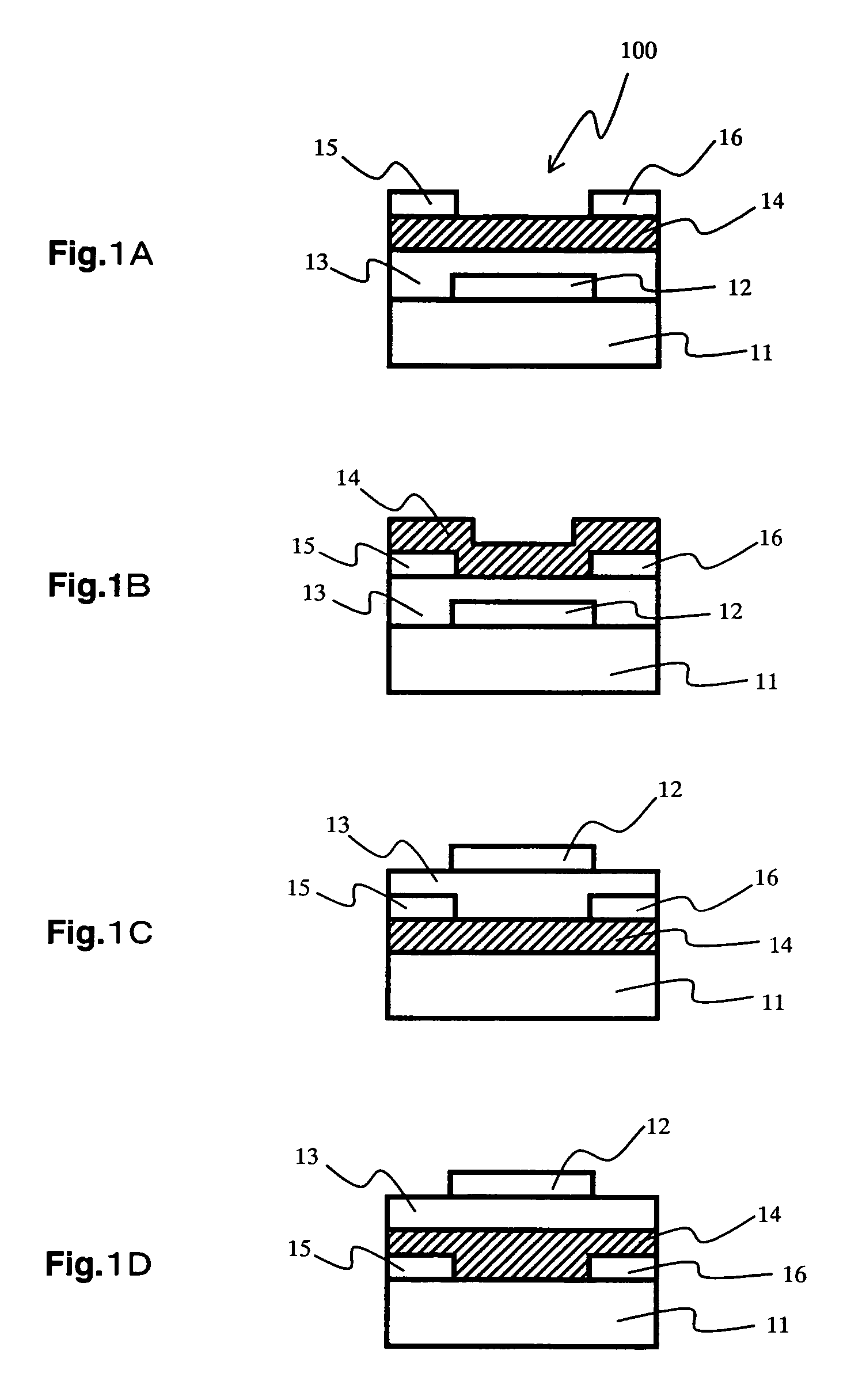
[0046]FIG. 1 is cross-sectional views schematically illustrating first representative configurations of TFTs.

[0047]As illustrated in FIGS. 1A to 1D, various configurations are conceived as the configuration of a TFT 100 according to the present embodiment. In all the configurations, the TFT is furnished with a substrate 11, a gate electrode 12, a gate insulating layer 13, a semiconductor layer 14, a source electrode 15, and a drain electrode 16. Generally, the configurations of FIGS. 1A and 1B are referred to as the bottom gate design. On the other hand, the configurations of FIGS. 1C and 1D are referred to as the top gate design. At the same time, because of the positional relationship of the semiconductor layer 14 with the source electrode 15 and the drain electrode 16, ...

second embodiment

[0072]A second embodiment of the present invention describes a case in which pentacene is used as the π-conjugated organic semiconductor molecules that constitute the semiconductor layer of a TFT.

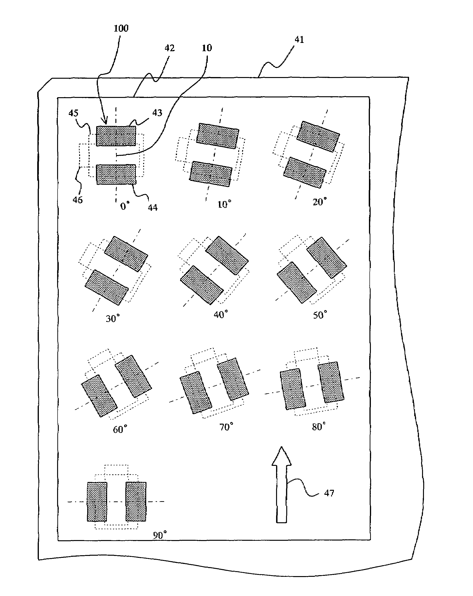
[0073]The present embodiment employs a TFT 100 having the configuration shown in FIG. 1B. It should be noted that the advantageous effects of the present invention are obtained by controlling the orientation direction of the semiconductor layer to be in an orientation with an appropriate angle with respect to the substrate plane. Therefore, the configuration of the TFT 100 itself is not limited to that shown in FIG. 1B.

[0074]As illustrated in FIG. 1B, the TFT 100 employing the bottom gate design has a substrate 11, a gate electrode 12, a gate insulating layer 13, a source electrode 15, a drain electrode 16, and a semiconductor layer 14 made of π-conjugated organic semiconductor molecules. Specifically, the gate electrode 12 is provided on the major surface of the substrate 11, and the gate ...

third embodiment

[0093]A third embodiment of the present invention describes a sheet-like flexible display, a wireless ID tag, and a portable device such as a portable television, a telecommunication terminal, and a portable medical device, as application examples that use the TFTs described in the first and second embodiments.

[0094]First, an example of the configuration of an active matrix-type display that employs an organic EL for its display unit will be described as the sheet-like flexible display.

[0095]FIG. 11 is a perspective view schematically illustrating the configuration of an active matrix-type display that uses an organic EL as its display unit, according to the present embodiment.

[0096]As illustrated in FIG. 11, the active matrix-type display according to the present embodiment has a TFT driving circuit 110 that is arranged on a plastic substrate 101 in an array form and is connected to pixel electrodes, and an organic EL layer 102 and a protective film 104 are arranged on the TFT driv...


PUM

PropertyMeasurementUnit
temperatureaaaaaaaaaa
gate voltageaaaaaaaaaa

Abstract

A thin film transistor of the present invention is a thin film transistor (100) having a semiconductor layer (14), a source region (15) and a drain region (16) provided to be isolated from each other so as to mutually oppose the semiconductor layer. The semiconductor layer has π-conjugated organic semiconductor molecules as its main component. The π-conjugated organic semiconductor molecules are oriented so that π orbitals substantially oppose each other and that the molecular axis of the main chains is oriented to be inclined with respect to a direction of electric field in a channel formed in the semiconductor layer.

Description

[0001]This application is the U.S. National Phase under 35 U.S.C. § 371 of International Application No. PCT / JP2004 / 010759, filed on Jul. 22, 2004, which in turn claims the benefit of Japanese Application No. 2003-381294, filed on Nov. 11, 2003, the disclosures of which Applications are incorporated by reference herein.TECHNICAL FIELD[0002]The present invention relates to thin film transistors and methods of fabricating the same. More particularly, the invention relates to a thin film transistor employing as a semiconductor layer a π-conjugated organic semiconductor that is orientation-formed, and to a method of fabricating the same.BACKGROUND ART[0003]At present, thin film transistors (hereinafter referred to as “TFTs”) are suitably used for driving elements in such devices as active matrix-type liquid crystal displays. Various configurations have been proposed as the configuration of the TFT, but a basic configuration is as follows; electric current flowing between a source electr...

Claims


Application Information

Patent Timeline
Patent Type & Authority Patents(United States)
IPC IPC(8): H01L35/24H01L51/00H01L51/05H01L51/30H01L51/40
CPCH01L51/0012H01L51/0036H01L51/0052H01L51/0541H01L51/0545H10K71/191H10K85/113H10K85/615H10K10/464H10K10/466
Inventor TAKEUCHI, TAKAYUKINANAI, NORISHIGE
Owner PANASONIC CORP
Why Eureka
Try Eureka