

Depleted sidewall-poly LDD transistor
- Summary
- Abstract
- Description
- Claims
- Application Information
AI Technical Summary
Benefits of technology
Problems solved by technology
Method used
Image

Examples
Embodiment Construction
Reference is now made in detail to a specific embodiment of the present invention, which illustrates the best mode presently contemplated by the inventor for practicing the invention. Alternative embodiments are also briefly described as applicable.
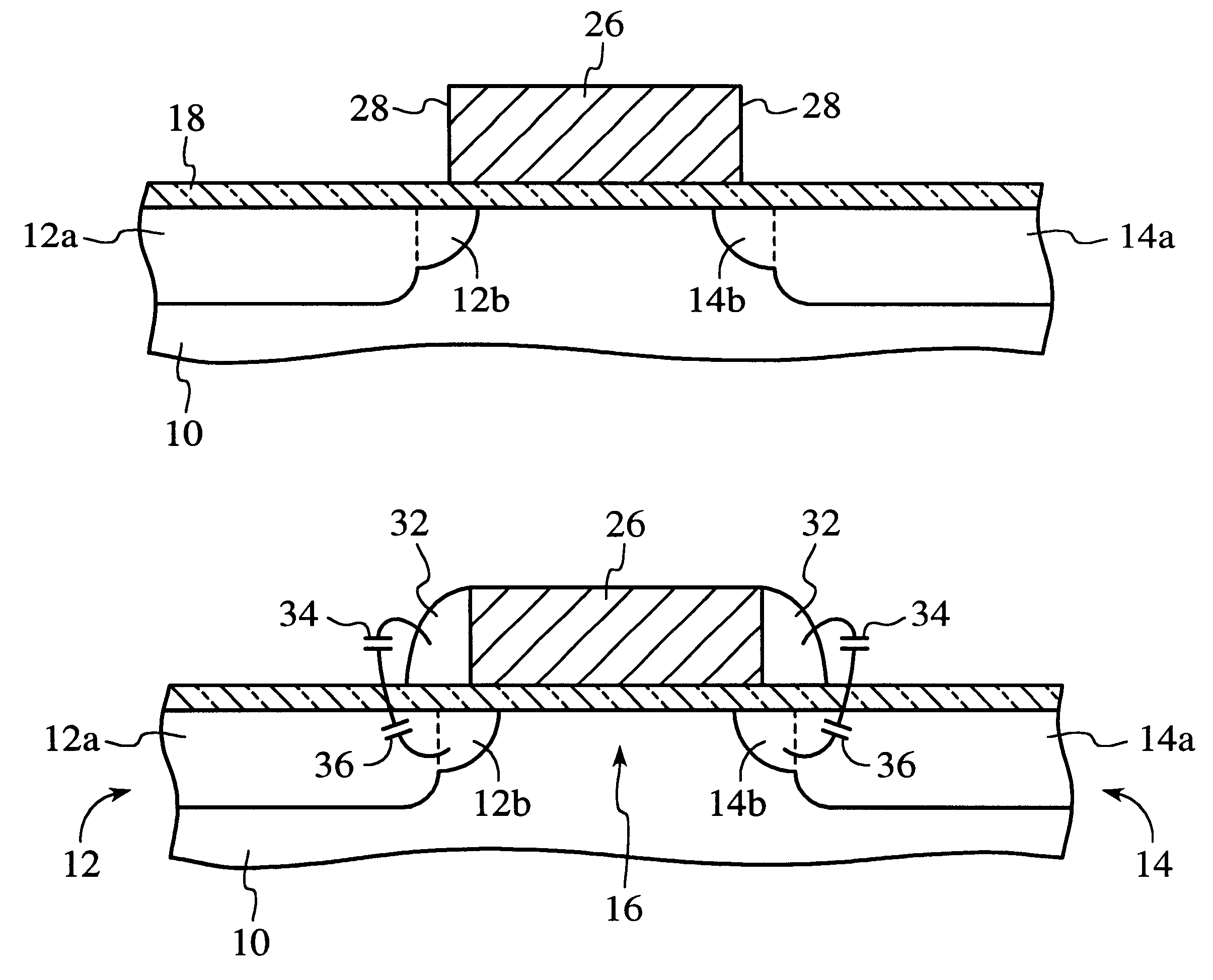
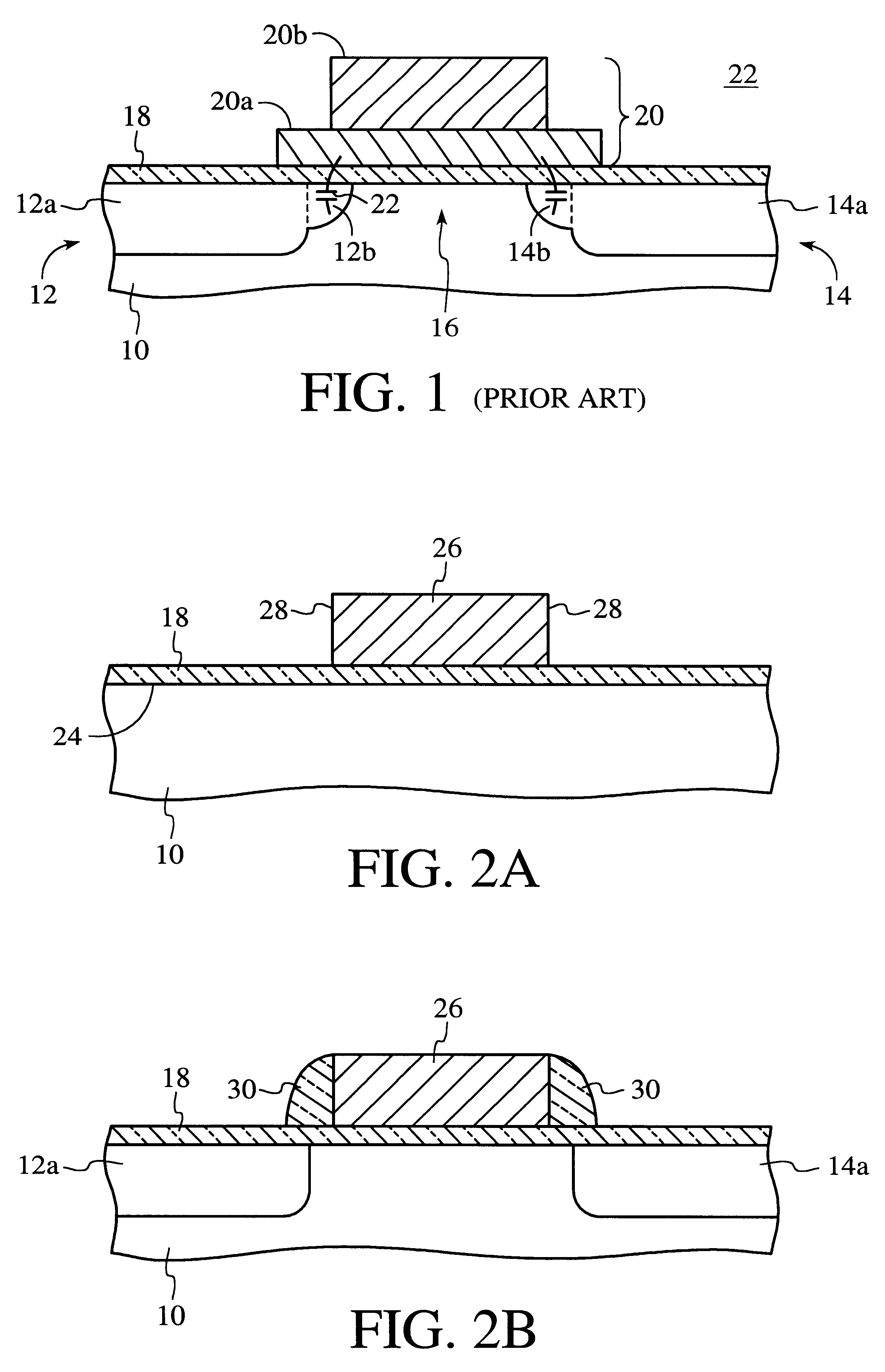
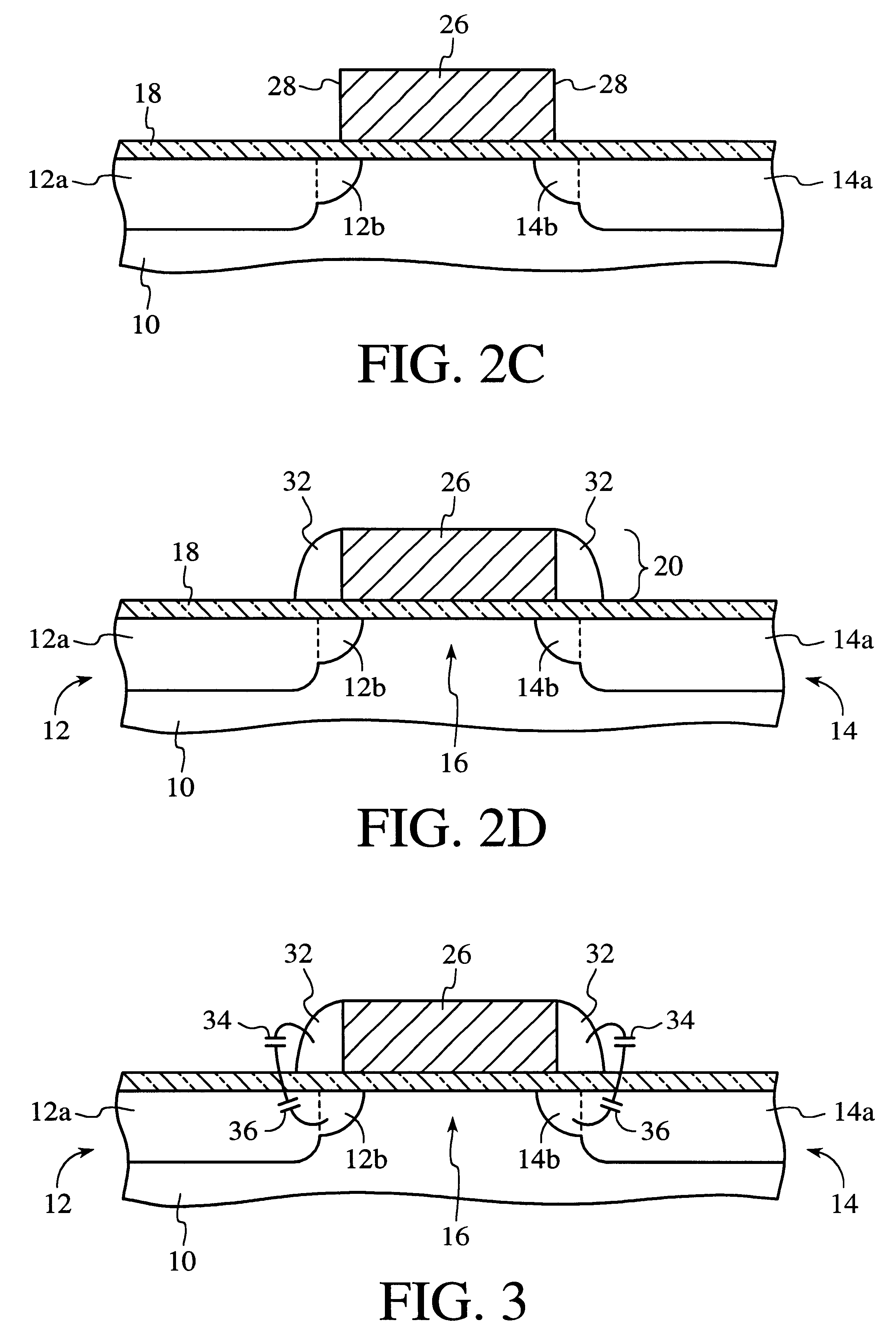
The present invention is directed to a metal oxide semiconductor transistor having a fully overlapped lightly doped drain (LDD) structure, which offers the advantages of conventional fully overlapped LDD transistors, but, which significantly reduces the drain-to-gate overlap capacitance associated therewith.
To achieve fully overlapped LDD construction and reduced drain-to-gate overlap capacitance, the metal oxide semiconductor transistor of the present invention employs a gate electrode comprising a main gate region formed from heavily doped polysilicon and depleted sidewall polysilicon spacers formed from undoped polysilicon. In the MOS transistor of the present invention, the lightly doped regions are fully overlapped by the depleted si...
PUM
 Abstract
Description
Claims
Application Information