Precision BEOL resistors

Active Publication Date: 2019-06-25
IBM CORP
View PDF17 Cites 0 Cited by
  • Summary
  • Abstract
  • Description
  • Claims
  • Application Information

AI Technical Summary

Benefits of technology

[0005]A semiconductor structure that includes a resistor that is located within an interconnect dielectric material layer of an interconnect level is provided. In accordance with the present application, the resistor comprises a diffusion barrier material that is present at a bottom of a feature that is located in the interconnect dielectric material layer. In some embodiments, the resistor has a topmost surface that is located entirely beneath a topmost surface of the interconnect dielectric material layer. In such an embodiment, the resistor is provided by removing sidew

Problems solved by technology

Prior art methods of forming thin film resistors embedded in an interconnect dielectric material are complicated and expensive.
Moreover, topography issues arise when embedding a thin film resistor in an interconnect dielectric mat

Method used


Image

  • Precision BEOL resistors
  • Precision BEOL resistors
  • Precision BEOL resistors

Examples


first embodiment

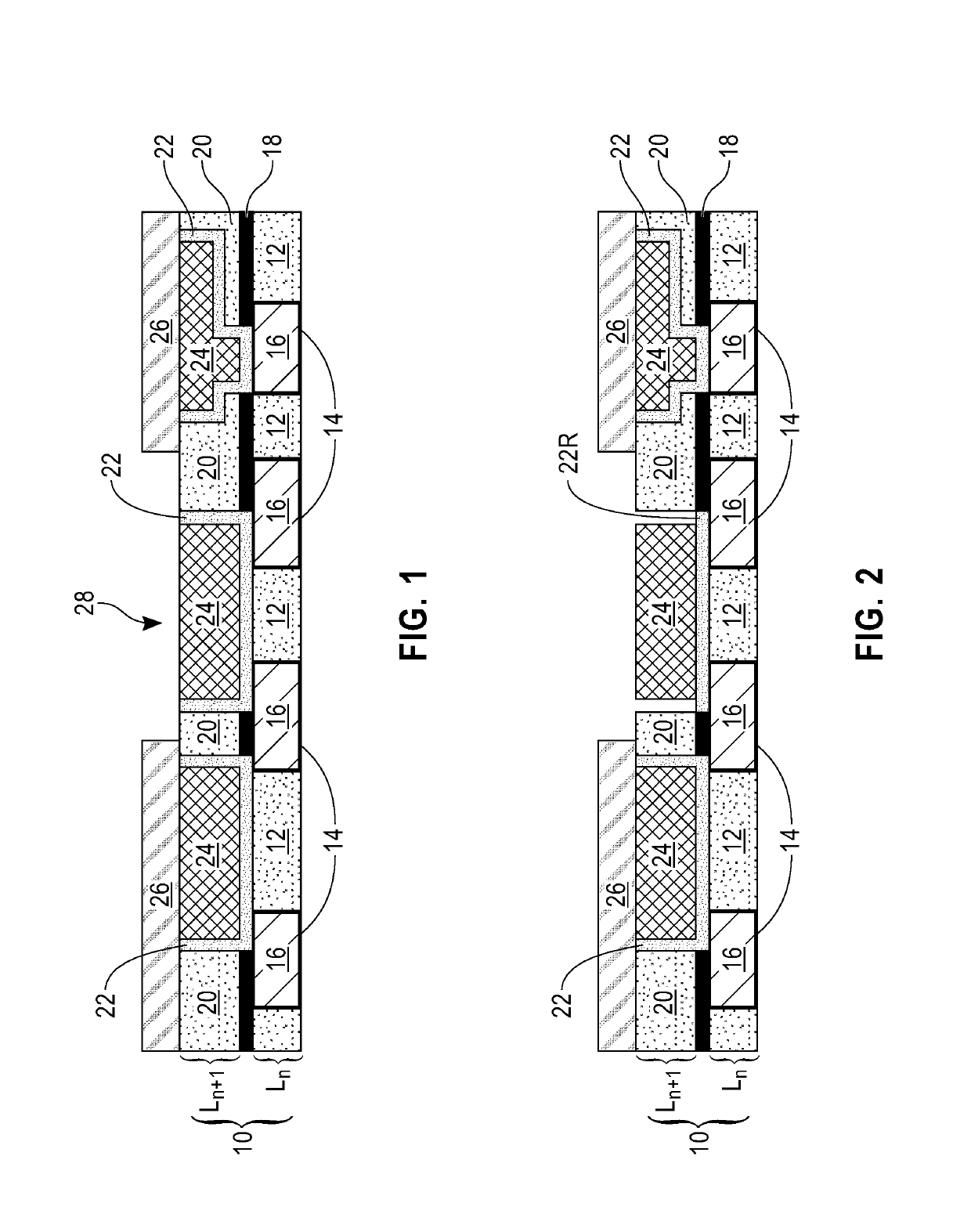
[0024]Referring first to FIG. 1, there is illustrated an exemplary semiconductor structure during an early stage of fabrication and in accordance with the present application. The exemplary semiconductor structure shown in FIG. 1 includes a patterned hard mask 26 that is formed on an upper interconnect level, Ln+1, of an interconnect structure 10. The patterned hard mask 26 includes an opening 28 that physically exposes an area of the upper interconnect level, Ln+1, in which a precision BEOL resistor in accordance with the present application will be subsequently formed. The patterned hard mask 26 covers interconnect device areas of the exemplary structure, i.e., areas in which interconnect metal-containing structures are to remain. The upper interconnect level, Ln+1, is located above a lower interconnect level Ln. In the present application, n is an integer starting at 1. In the illustrated embodiment, capping layer 18 is positioned between the lower interconnect level, Ln, and the...

second embodiment

[0057]Referring now to FIG. 7, there is illustrated an exemplary semiconductor structure during an early stage of fabrication in accordance with the present application. The exemplary structure of FIG. 7 includes a capping layer 56 that is located on an interconnect level, Ln. The interconnect level, Ln, of this embodiment of the present application includes an interconnect dielectric material layer 50 having a metal-containing structure 54 embedded therein. As is shown, a diffusion barrier liner 52 is present on the sidewalls and along a bottom wall of the metal-containing structure 54 thus separating the metal-containing structure 54 from the interconnect dielectric material layer 50. The diffusion barrier liner 52 and the metal-containing structure 54 have topmost surfaces that are coplanar with each other as well as being coplanar with a topmost surface of the interconnect dielectric material layer 50.

[0058]The interconnect dielectric material layer 50 of this embodiment of the ...


PUM


Abstract

A semiconductor structure that includes a resistor that is located within an interconnect dielectric material layer of an interconnect level is provided. The resistor includes a diffusion barrier material that is present at a bottom of a feature that is located in the interconnect dielectric material layer. In some embodiments, the resistor has a topmost surface that is located entirely beneath a topmost surface of the interconnect dielectric material layer. In such an embodiment, the resistor is provided by removing sidewall portions of a diffusion barrier liner that surrounds a metal-containing structure. The removal of the sidewall portions of the diffusion barrier liner reduces the parasitic noise that is contributed to the sidewall portions of a resistor that includes such a diffusion barrier liner. Improved precision can also be obtained since sidewall portions may have a high thickness variation which may adversely affect the resistor's precision.

Description

BACKGROUND[0001]The present application relates to a semiconductor structure and a method of forming the same. More particularly, the present application relates to back-end-of-the-line (BEOL) resistors that have high precision as well as methods of forming such BEOL resistors.[0002]A resistor, which is a passive two-terminal electrical component that implements electrical resistance as a circuit element, is one of the most common electrical components present in almost every electrical device. In electronic circuits, resistors can be used to limit current flow, to adjust signal levels, bias active elements, and terminate transition lines.[0003]In semiconductor devices, it is well known to have a thin film resistor such as, for example, a resistor composed of TaN, embedded in the chip through either a damascene approach or a subtractive etch method. For example, and during back-end-of-the-line (BEOL) processing, a thin film resistor may be embedded in an interconnect dielectric mate...

Claims


Application Information

Patent Timeline
IPC IPC(8): H01L23/522H01L49/02H01L21/48
CPCH01L28/20H01L23/5228H01L21/485
Inventor LI, BAOZHENPETERSON, KIRKSHEETS, JOHNCLEVENGER, LAWRENCE A.WANG, JUNLIYANG, CHIH-CHAO
Owner IBM CORP
Why Eureka
Try Eureka