Etching mask, method of making same, etching method, magnetic head device and method of manufacturing same

a technology of mask and etching method, which is applied in the manufacture of flux-sensitive heads, instruments, and record information storage, etc., can solve the problems of reducing the etching speed of the mask, not only the workpiece to be etched, but also the mask itsel

Inactive Publication Date: 2001-10-16
TDK CORPARATION
View PDF5 Cites 10 Cited by
  • Summary
  • Abstract
  • Description
  • Claims
  • Application Information

AI Technical Summary

Problems solved by technology

One of problems found in such an etching process is that not only the workpiece to be etched but also the mask itself is etched.
However, an increased film thickness makes it difficult to maintain anisotropy of etching, which is not desirable for fine pattern fabrication.
However, if a metal mask is used, a problem still remains, that is, the top and sidewall surface of the mask are removed together with the workpiece through an ion beam application although the etching speed of the mask is decreased. FIG. 14A to FIG. 14C illustrate such a state.
In a composite thin film magnetic head device as mentioned above, in particular, if the cross section of a writing pole formed on a gap layer takes the

Method used


Image

  • Etching mask, method of making same, etching method, magnetic head device and method of manufacturing same
  • Etching mask, method of making same, etching method, magnetic head device and method of manufacturing same
  • Etching mask, method of making same, etching method, magnetic head device and method of manufacturing same

Examples


Embodiment Construction

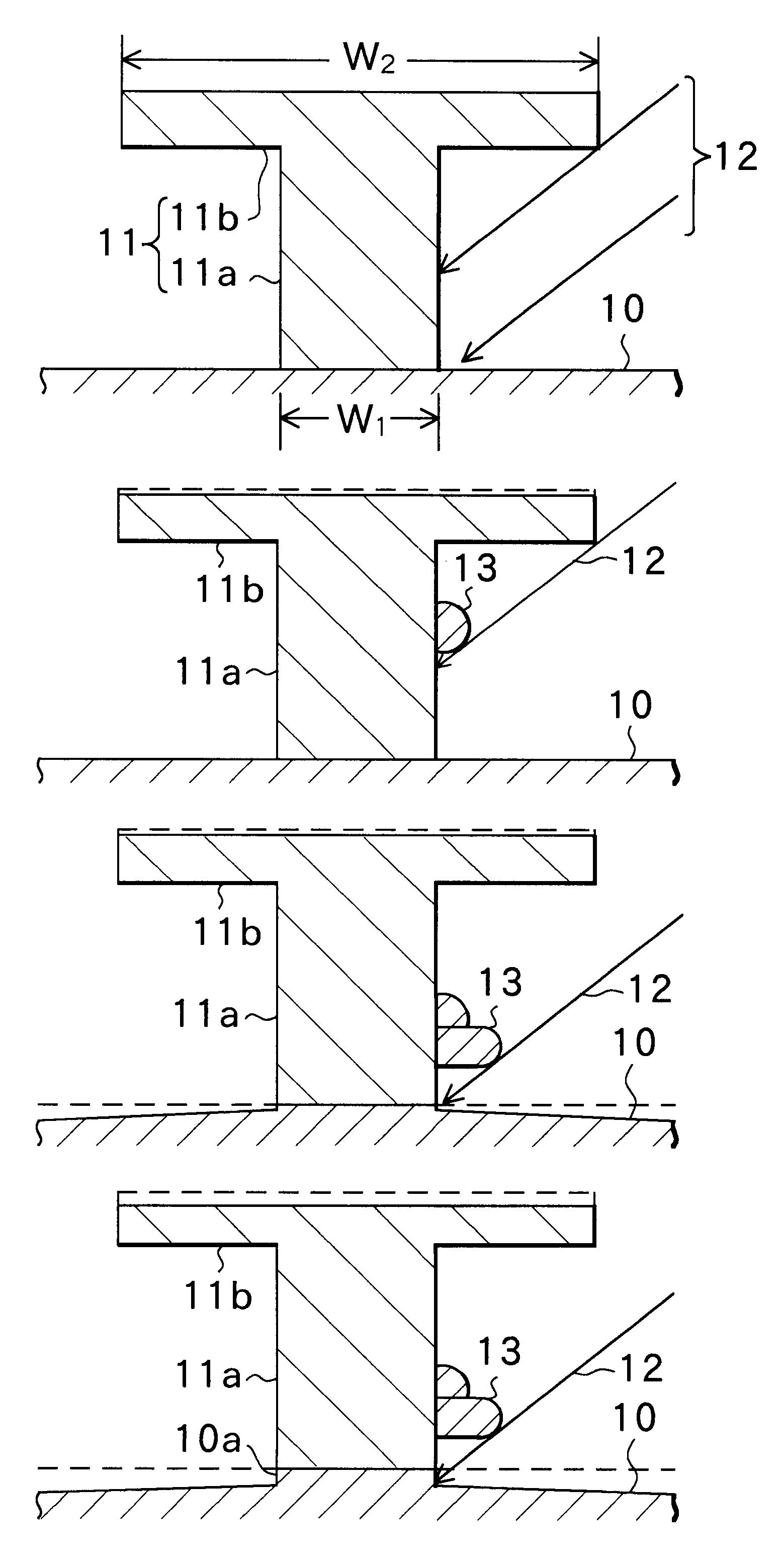
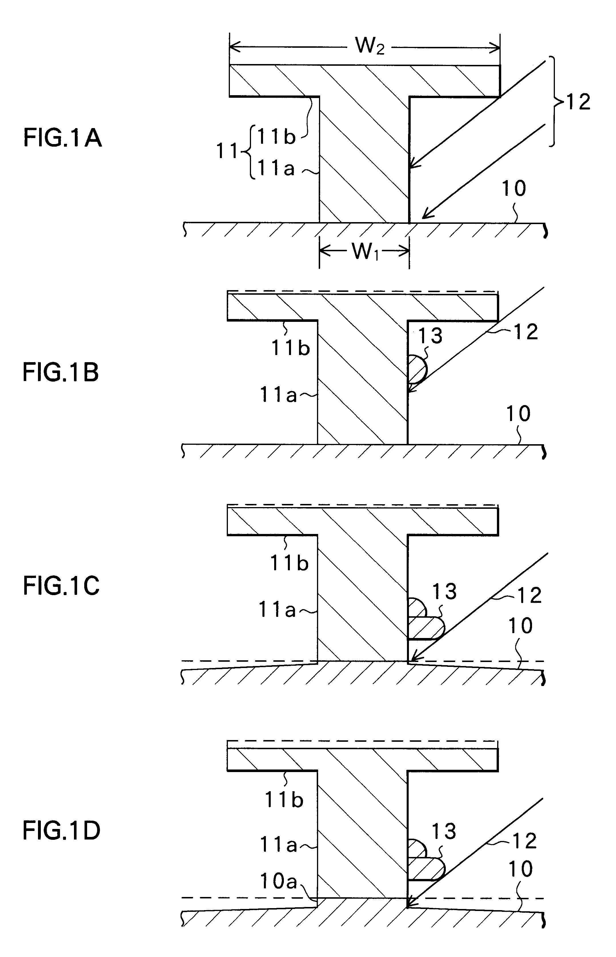
An etching mask was formed through the first method shown in FIG. 3A to FIG. 3E. A resist pattern having an opening of 5.0 .mu.m in thickness and 1.0 .mu.m in width was formed on a semiconductor wafer on which an electrode layer was formed, the electrode layer including three layers of a NiFe (18 weight % of Ni) film (0.5 .mu.m in thickness), a SiO.sub.2 film (0.25 .mu.m in thickness), and a NiFe (18 weight % of Ni) film (0.5 .mu.m in thickness). Plating was then performed. As pretreatment, the wafer was immersed in a 4.5% hydrochloric acid (HCl) solution for about 2 minutes. Next, the wafer was immersed in a dilute plating solution of pure water (NiB electroless plating solution) of pH 6.0 whose temperature was maintained at 50.degree. C. for 25 minutes. A plating film of 2.0 .mu.m in thickness was thus formed. The formula of the plating film was 99% of Ni and 1% of B. Ion beam etching was then performed, using the etching mask made of the plating film, until the three layers of th...


PUM

PropertyMeasurementUnit
Thicknessaaaaaaaaaa
Widthaaaaaaaaaa
Depthaaaaaaaaaa

Abstract

An etching mask is made of a metal such as Permalloy (NiFe) and has a T-shaped cross section made up of a vertical bar having width W1 and a lateral bar having width W2. Through ion beam etching with the etching mask, the region in the surface of a workpiece not covered with the mask is selectively removed by the ion beams applied thereto. In the mask the vertical bar has a region obstructed by the lateral bar and a redeposit portion. As a result, the region of the vertical bar near the interface between the workpiece and the vertical bar that substantially determines the pattern width does not change in width. Consequently, a pattern of the workpiece on which etching has been performed has the top width and bottom width substantially equal to width W1 of the vertical bar of the mask. The pattern is rectangular in cross section.

Description

1. Field of the InventionThe present invention relates to an etching mask used for micromachining, a method of making the same, an etching method using the etching mask, a magnetic head device and a method of manufacturing the same, which are used for making writing poles and so on of a composite thin-film magnetic head device having a reading head and a writing head, for example.2. Description of the Related ArtDemands have been increasing for techniques that achieve finer patterns as a reduction has been sought in size and film thickness of a magnetic head device such as a magnetoresistive (MR) head device used for a hard disk unit and various semiconductor devices. Fabrication of a micropattern includes an etching process. Anisotropic etching is required for achieving high etching accuracy in the etching process. Anisotropic etching has such orientation that a sidewall surface of a complete pattern is orthogonal to the surface of a base layer. An example that requires anisotropic...

Claims


Application Information

Patent Timeline
IPC IPC(8): G11B5/31G11B5/39C23F4/00H01L21/302H01L21/3065
CPCG11B5/3116G11B5/3163G11B5/312G11B5/3967Y10S438/975Y10S438/942
Inventor MATSUKUMA, KOJI
Owner TDK CORPARATION
Why Eureka
Try Eureka