

Mounting structure for semiconductor device
a superconductor and mounting structure technology, applied in the direction of superconducting magnets/coils, magnetic bodies, waveguides, etc., can solve the problems of low electric resistance, superconductive phenomena, and the inability to pump sealed gas ou
- Summary
- Abstract
- Description
- Claims
- Application Information
AI Technical Summary
Problems solved by technology
Method used
Image

Examples
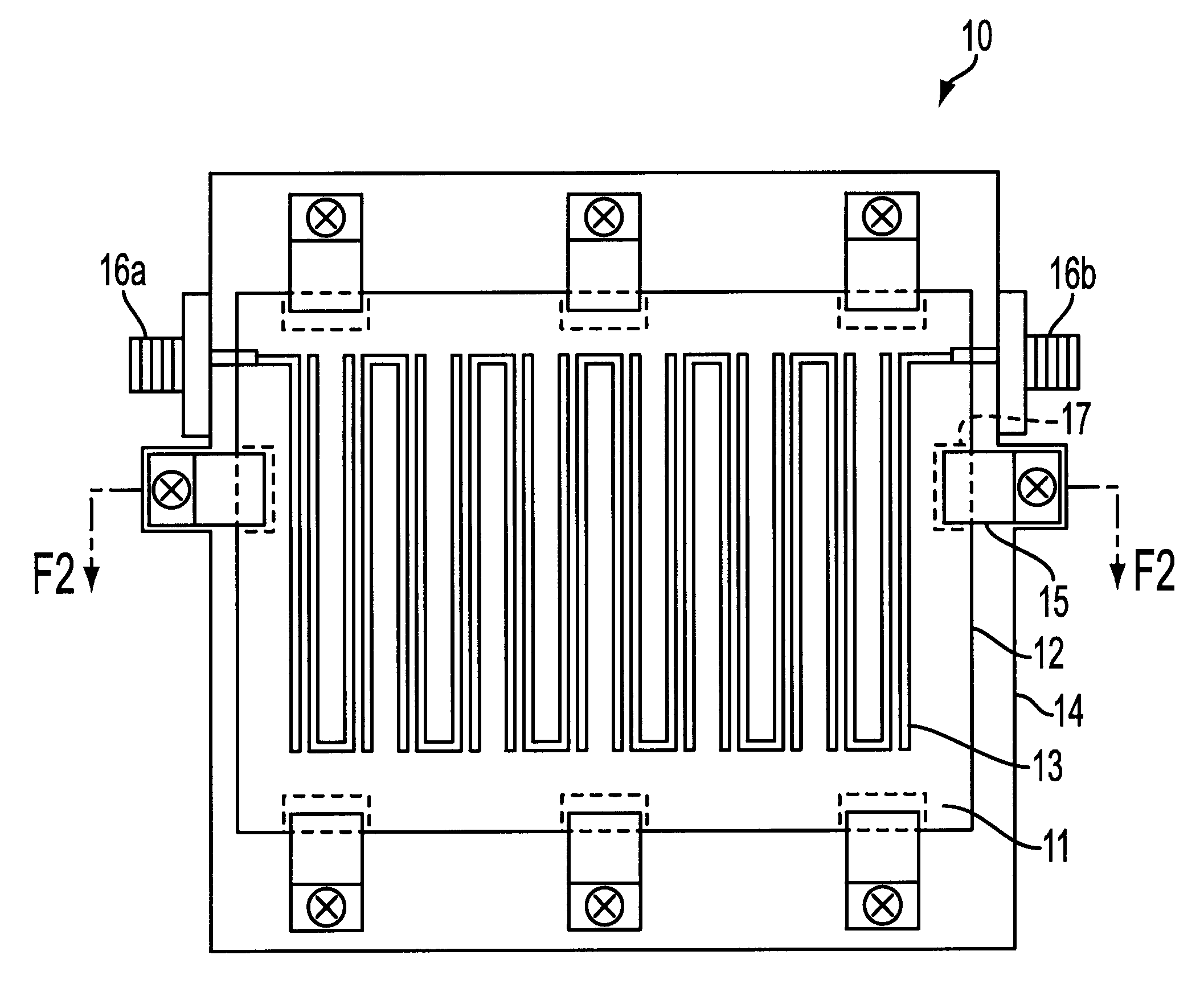
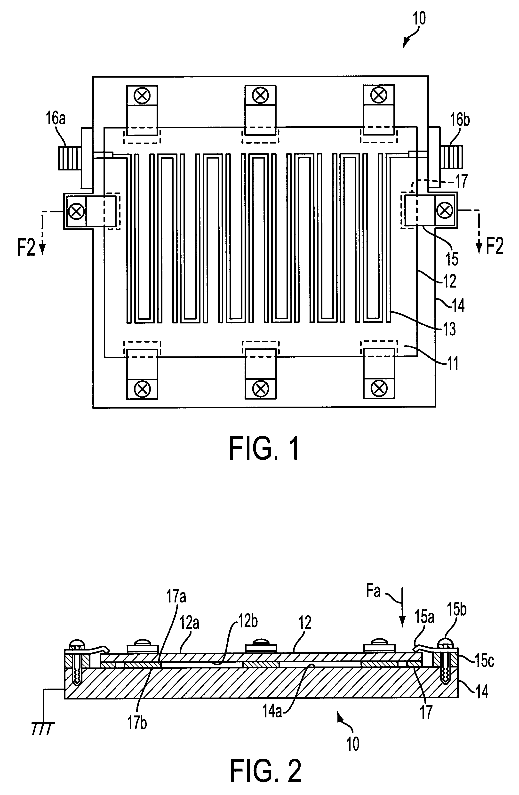
first embodiment
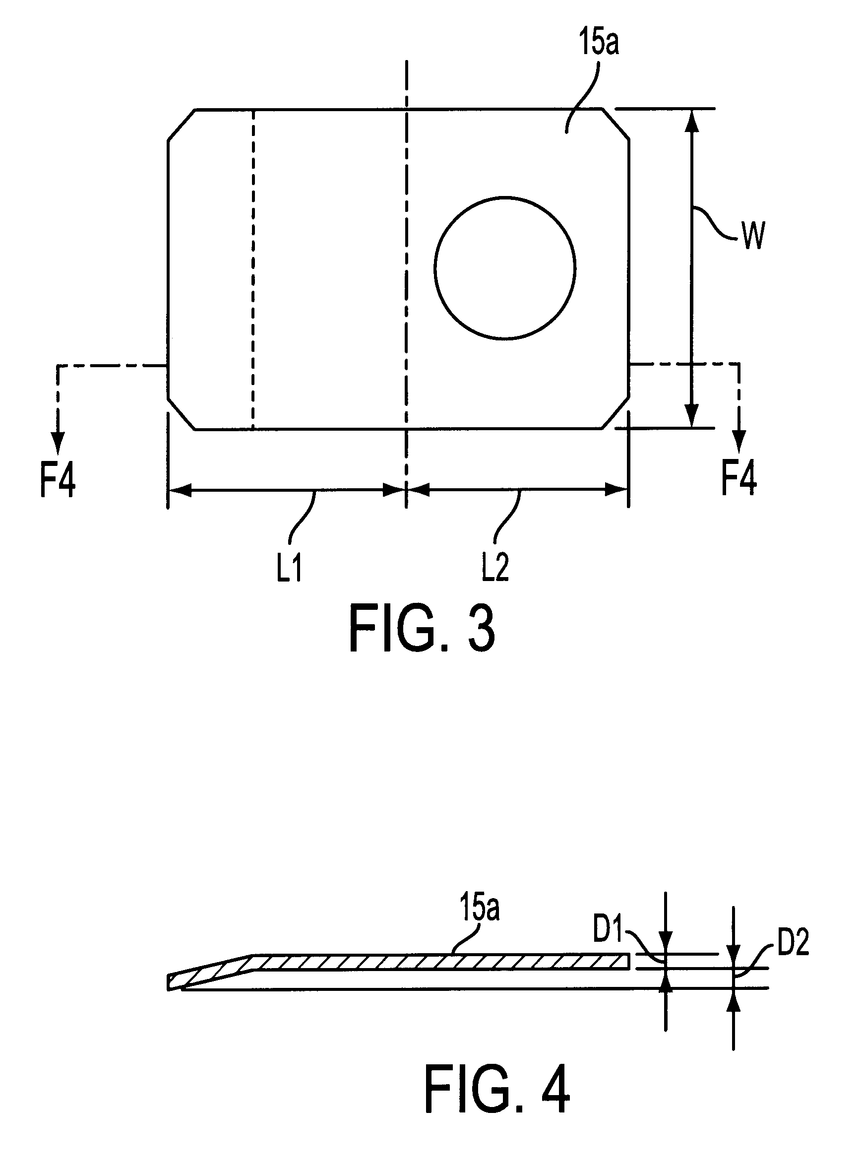
Although the conductive layer 17 made of a gold foil is placed between the dielectric substrate 12 and the device holder 14 in the first embodiment, the conductive layer 17 may be constructed through the other processes which will be described hereinlater with reference to FIGS. 5 and 6 of the drawings.
In one of the processes of forming the conductive layer 17, as shown in FIG. 5, the conductive layer 17 is integrated with the ground layer of the filter 11, i.e., the side of second surface 12b of the dielectric substrate 12, through a general physical vapor deposition method. Therefore, the first surface 17a of the conductive layer 17 can be held in hermetical contact with the ground layer of the filter 11 i.e., the side of the second surface 12b of the dielectric substrate 12.
In the other of the processes of forming the conductive layer 17, as shown in FIG. 6, the conductive layer 17 is integrated with the base surface 14a of the device holder 14 through a general physical vapor de...
second embodiment
Referring now to FIGS. 7 and 9 of the drawings, there is shown the mounting structure 20 for the superconductor device according to the present invention. In this embodiment, the mounting structure 20 is adaptable for mounting a planer band-pass filter 21 and contained in the device holding apparatus 1 shown in FIG. 13, when the superconductor device 4 is operated under the specific condition, i.e., at the pressure of 2.times.10.sup.-2 Pa or less in the closed vacuum chamber and at the temperature of 80 K or less.
The filter 21 is adapted to have a signal inputted from a first external device (not shown in the drawings) to output a second external device (not shown). The filter 21 should have a filter function in frequency response defined as the attenuation A of 90 dB or more. As shown in FIGS. 7 and 8, the filter 21 comprises a dielectric substrate 22 having first and second surfaces 22a and 22b diametrically opposite to each other and a circuit layer 23. The circuit layer 23 has a...
third embodiment
Referring now to FIGS. 10 and 11 of the drawings, there is shown the mounting structure 30 for the superconductor device according to the present invention. In this embodiment, the mounting structure 30 is adaptable for mounting a pair of planer band-pass filters 31a and 31b and contained in the device holding apparatus 1 shown in FIG. 13, when the superconductor device 4 is operated under the specific condition, i.e., at the pressure of 2.times.10.sup.-2 Pa or less in a closed vacuum chamber and at the temperature of 80 K or less.
The pair of filters 31a and 31b is arranged next to each other as shown in FIGS. 10 and 11. The filters 31a and 3b are identical to each other. Therefore, the filters 31a and 31b are representatively referred to as "the filter 31" in the following description when it is unnecessary to distinguish between the filters 31a and 31b.
The filter 31 is adapted to have a signal inputted from a first external device (not shown in the drawings) to output a second ext...
PUM
 Abstract
Description
Claims
Application Information