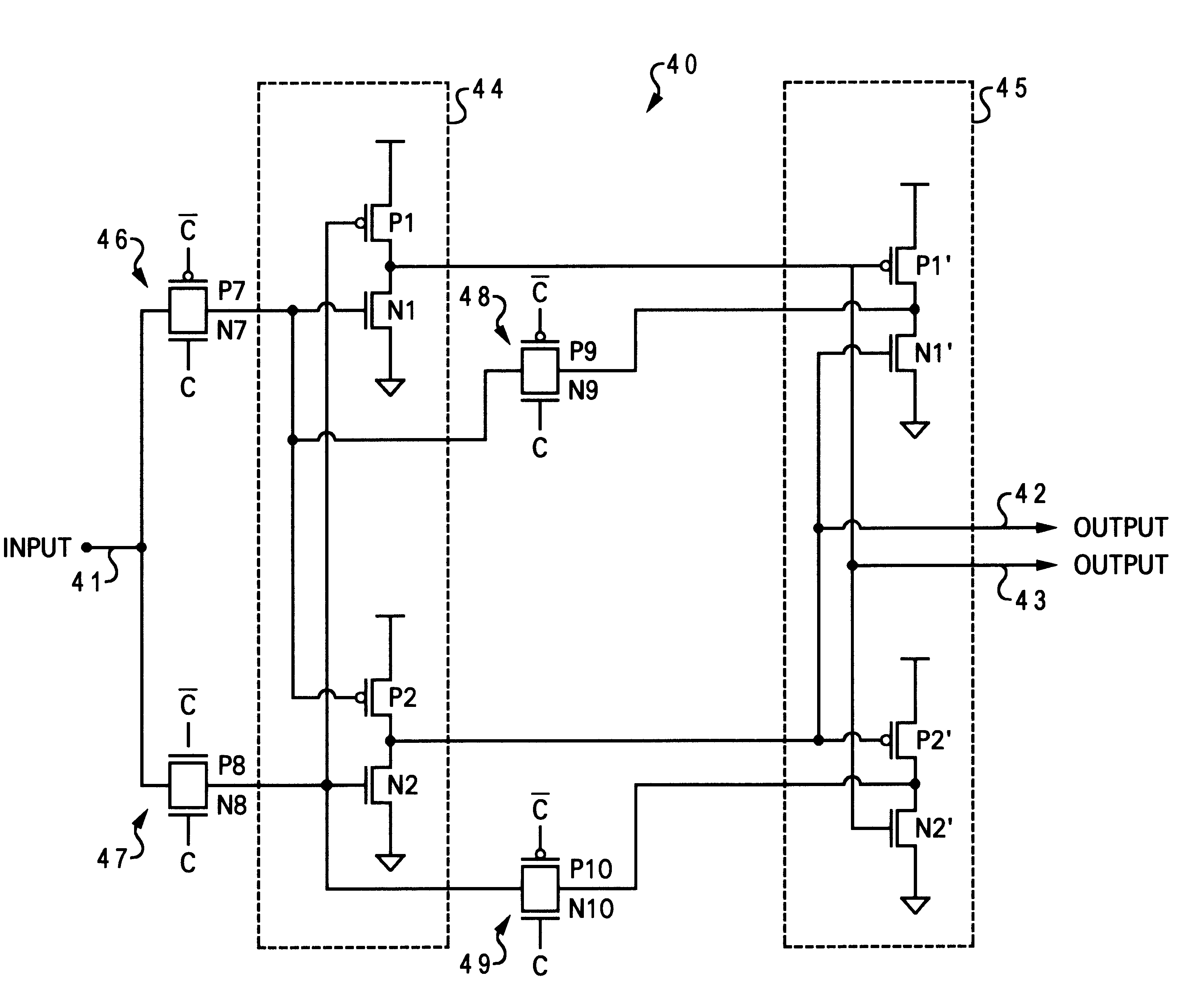
Single event upset (SEU) hardened latch circuit
a latch circuit and single event technology, applied in the field of latch circuits, can solve the problems of inability to adapt to the application, and inability to adapt to the environmen
- Summary
- Abstract
- Description
- Claims
- Application Information
AI Technical Summary
Problems solved by technology
Method used
Image
Examples
Embodiment Construction
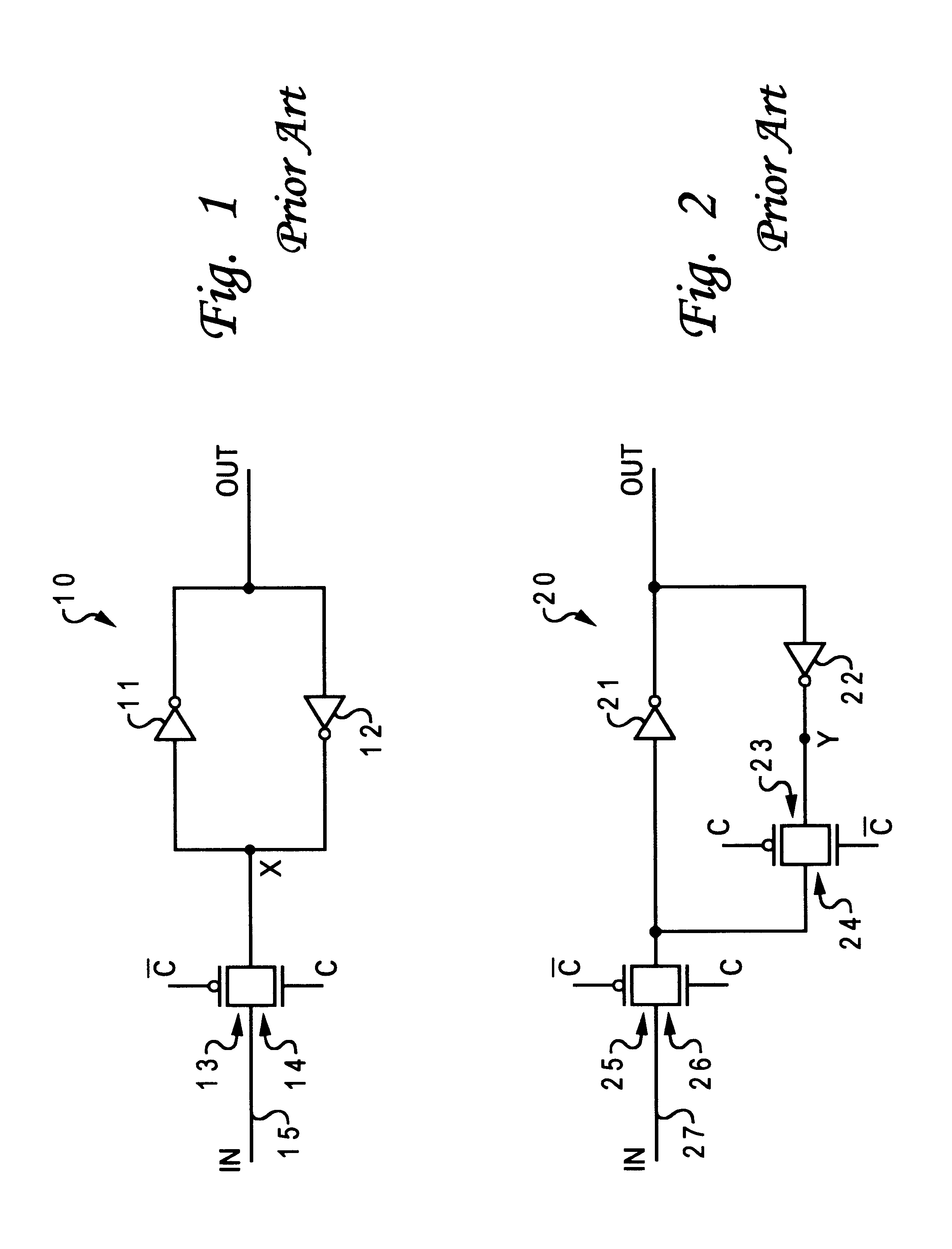
Referring now to the drawings and in particular to FIG. 1, there is illustrated a schematic diagram of a first latch circuit according to the prior art. As shown, a latch circuit 10 includes inverters 11, 12 and transistors 13, 14. The output of inverter 11 is connected to the input of inverter 12, and the output of inverter 12 is connected to the input of inverter 11. Such configuration allows a data value to be stored at a node x. The data value stored at node x can be changed by turning on transistors 13, 14, which are connected in a pass gate configuration, such that data at input 15 can be transmitted to node x.
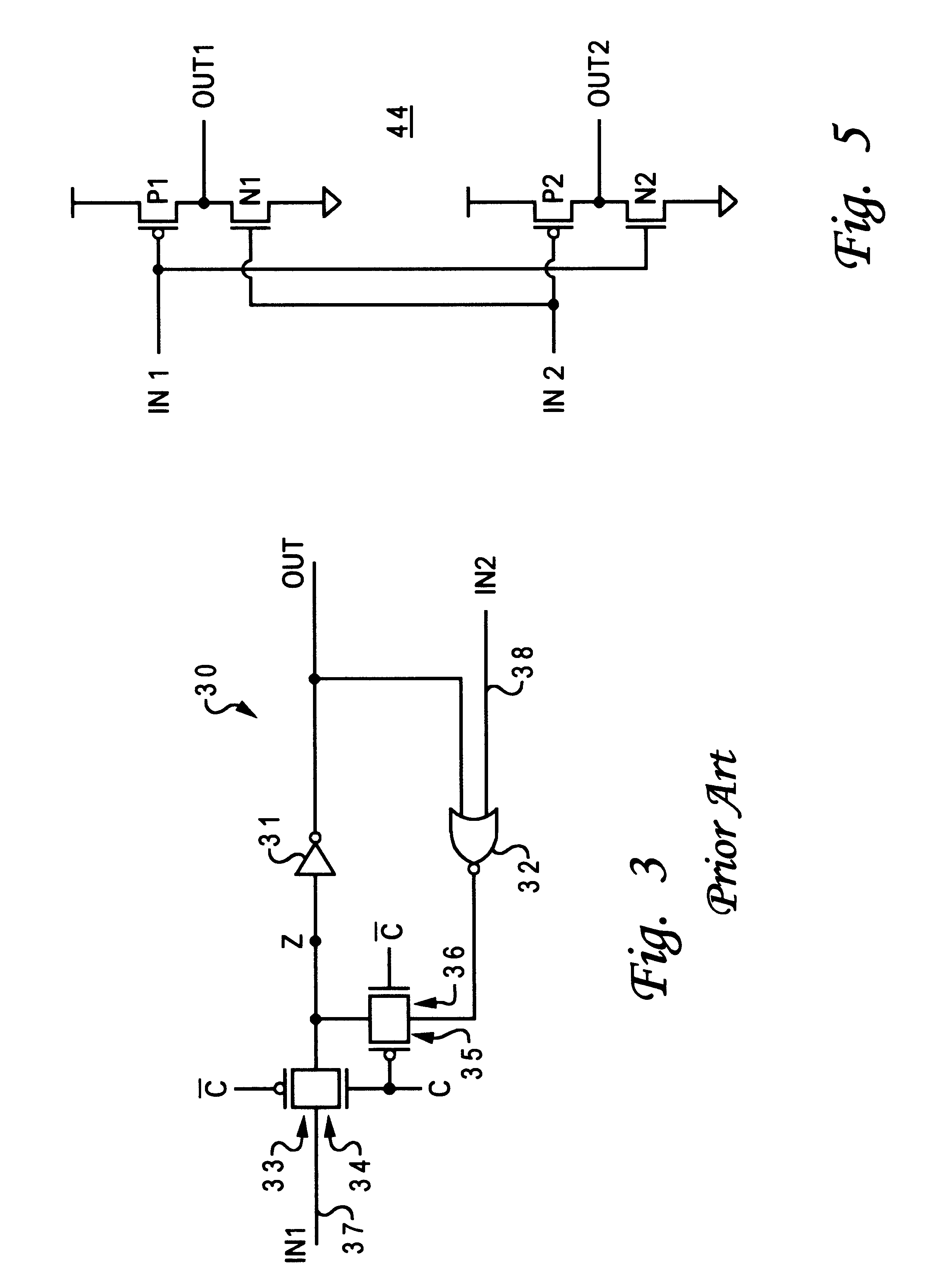
With reference now to FIG. 2, there is depicted a schematic diagram of a second latch circuit according to the prior art. As shown, a latch circuit 20 includes inverters 21, 22 and transistors 23-26. Similar to latch circuit 10 from FIG. 1, the output of inverter 21 is connected to the input of inverter 22. However, the output of inverter 22 is connected to the input of ...
PUM
 Abstract
Description
Claims
Application Information


