Method for fabricating a thin-film transistor

a thin-film transistor and fabrication method technology, applied in solid-state devices, material nanotechnology, semiconductor devices, etc., can solve the disadvantage of processing relying on vacuum evaporated conductors

Inactive Publication Date: 2001-12-11
BELL SEMICON LLC
View PDF3 Cites 111 Cited by
  • Summary
  • Abstract
  • Description
  • Claims
  • Application Information

AI Technical Summary

Problems solved by technology

Such methods, however, may have the processing disadvantage of relying on

Method used


Image

  • Method for fabricating a thin-film transistor
  • Method for fabricating a thin-film transistor
  • Method for fabricating a thin-film transistor

Examples


Embodiment Construction

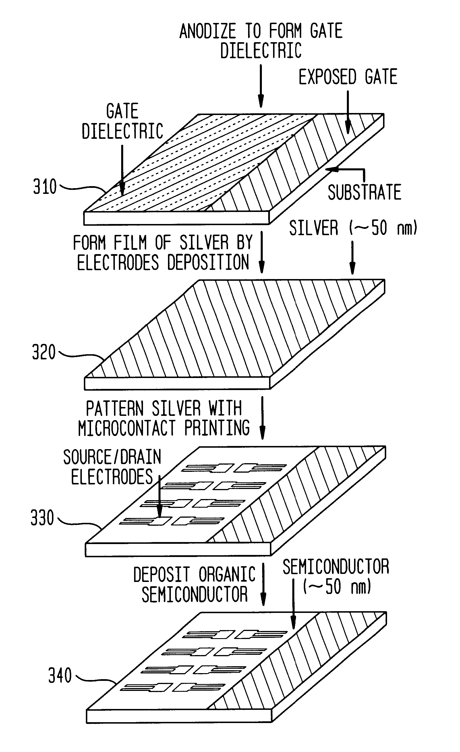
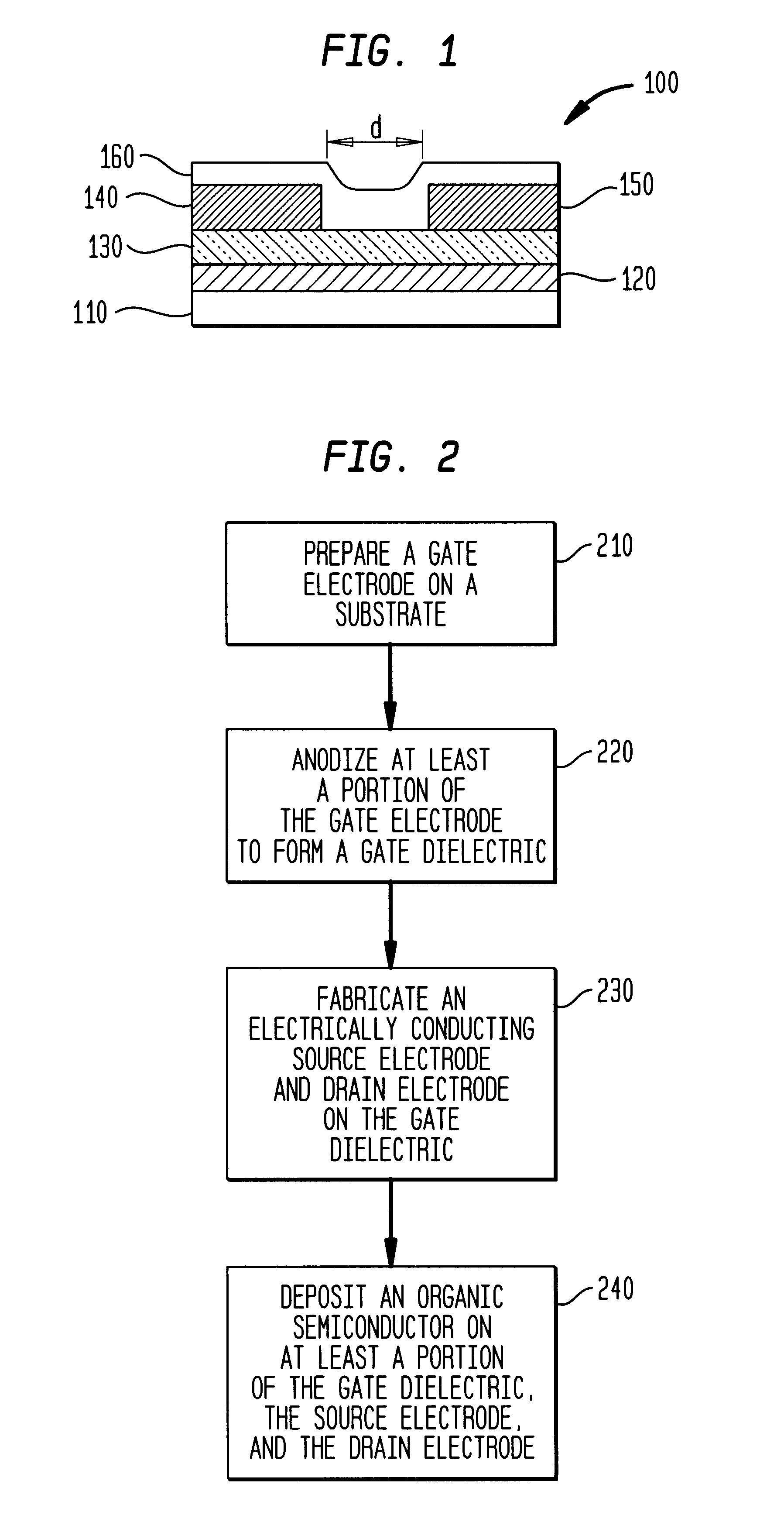
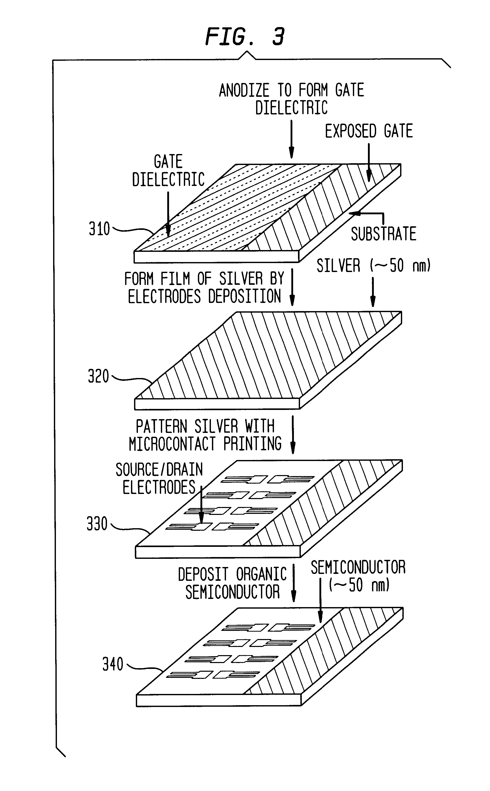
Preparing the Gate Electrode and Gate Dielectric

In an exemplary embodiment of the present invention, transistors of the present invention were fabricated using three dielectric / gate materials: (i) thermally grown SiO.sub.2 on a highly doped silicon substrate (n-type, .rho.=0.02-1.0 .OMEGA.cm, Silrec Corp.; wherein p is resistivity), (ii) anodically grown Ta.sub.2 O.sub.5 on sputtered tantalum on silicon and (iii) anodically grown SiO.sub.2 on highly doped silicon. The transistors with thermal SiO.sub.2, were constructed to establish the utility of microcontact printing on electroless silver for fabricating the source and drain electrodes. Microcontact printing with electroless silver deposited onto the anodized dielectrics yielded transistors having a comparable performance to devices that use thermal SiO.sub.2.

In an exemplary embodiment of the present invention, anodized Ta.sub.2 O.sub.5 was made from approximately 200 nm tantalum films sputter deposited on silicon (100) wafers. Th...


PUM

PropertyMeasurementUnit
Electrical conductoraaaaaaaaaa

Abstract

A method for fabricating a thin-film field effect transistor such as a thin-film field effect transistor. The method includes preparing a gate electrode on a substrate, anodizing at least a portion of the gate electrode to form a gate dielectric, and fabricating an electrically conducting source electrode and a drain electrode on the gate dielectric. The method also includes depositing an organic semiconductor on at least a portion of the gate dielectric, the source electrode and the drain electrode.

Description

The present invention relates to the field of thin-film transistors, in particular the field of fabricating an organic thin-film field effect transistor.BACKGROUND INFORMATIONTechniques for fabricating and patterning transistors include photochemical patterning, for example, to construct source / drain electrodes and appropriate interconnections for functional organic circuits. Such methods, however, may have the processing disadvantage of relying on vacuum evaporated conductors for source, drain and thin dielectric layers. Although it is possible to produce low voltage (.about.5 V) transistors with thin gate dielectrics of SiO.sub.2 (.about.100 nm) by combining printing and low cost near-field photolithographic methods, solution processed dielectrics typically include thick (.about.1 .mu.m) spin cast or screen printed polymer films. Accordingly, the low capacitance of these layers restricts operation to voltages (.about.100 V) that may exceed voltages required for many applications.H...

Claims


Application Information

Patent Timeline
IPC IPC(8): H01L51/40H01L51/05H01L21/02H01L21/316H01L51/30H01L21/336H01L51/00
CPCB82Y30/00H01L51/0021H01L51/0545H01L21/31687H01L51/0023H01L51/0036H01L21/02183H01L21/02186H01L21/02164H01L21/02189H01L21/02258H01L21/02175H01L21/02178H01L21/02181H10K71/60H10K71/621H10K85/113H10K10/466
Inventor JONES, CHRISTOPHER D. W.MURPHY, DONALD W.ROGERS, JOHN A.TATE, JENNIFERSLUSHER, RICHART E.
Owner BELL SEMICON LLC
Why Eureka
Try Eureka