Buffer circuit
a buffer circuit and circuit technology, applied in electronic switching, digital storage, instruments, etc., can solve the problems of unstable operation and/or malfunction of these circuits, large deviation or fluctuation of power supply voltage and ground voltage, and inability to be ignored
- Summary
- Abstract
- Description
- Claims
- Application Information
AI Technical Summary
Problems solved by technology
Method used
Image

Examples
first embodiment
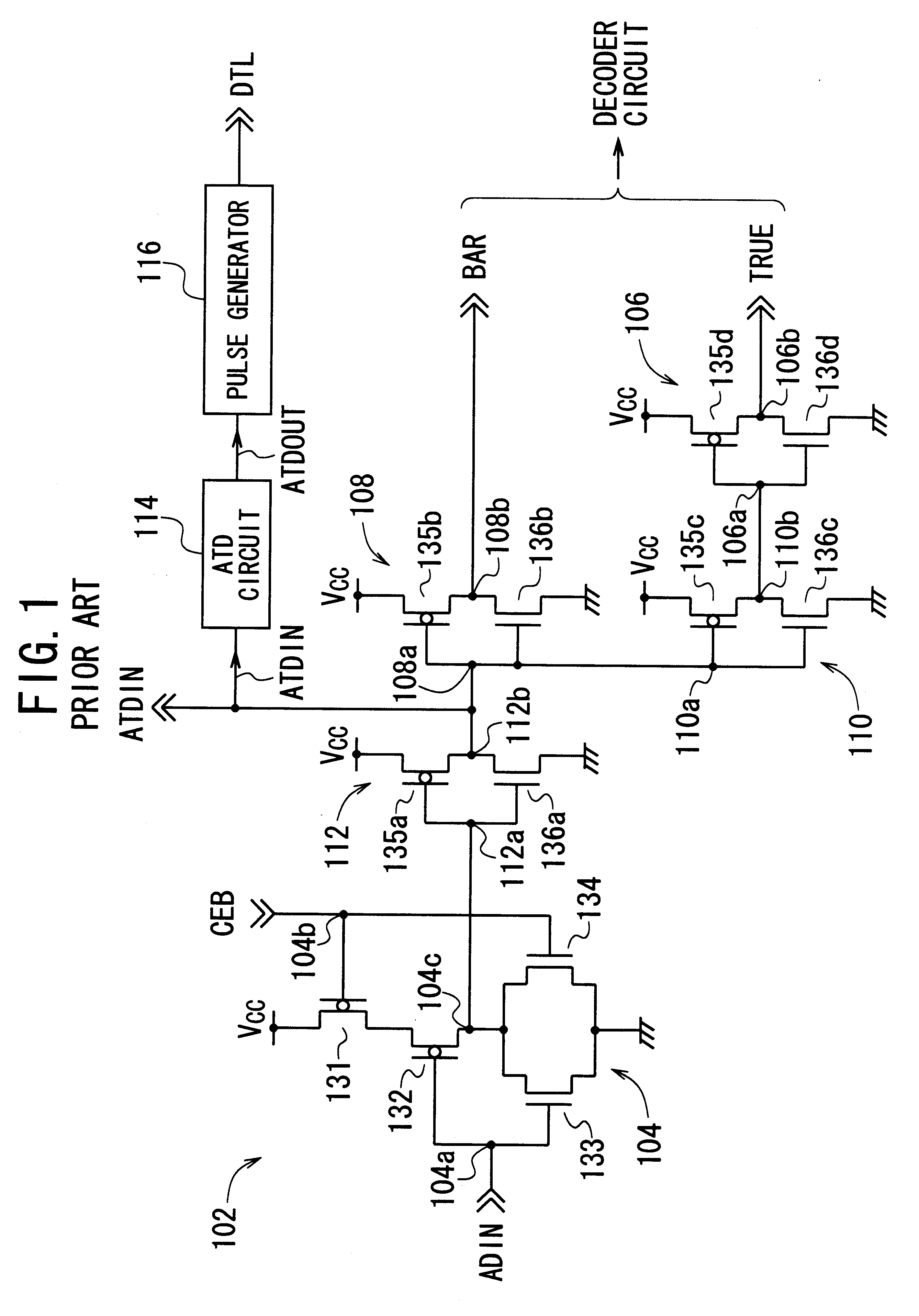
FIG. 3 shows an address buffer circuit according to the present invention, which is used for a semiconductor memory device.
The address buffer circuit 2 according to the first embodiment shown in FIG. 3 is comprised of an input stage 4, a first inverter circuit 6, a second inverter circuit 8, a third inverter circuit 10, a fourth inverter circuit 12, a fifth inverter circuit 14, an equalization circuit 16, an ATD circuit 18, a wave-synthesizing pulse generator circuit 20, a first latch circuit 22, and a second latch circuit 24. Only the configuration for one bit of address is shown in FIG. 3 for the sake of simplification; however, it is needless to say that the circuit 2 actually includes a lot of the same configuration as shown in FIG. 3 according to the bit count of address.
The input stage 4 is a two-input NOR gate comprising two p-channel MOSFETs 71 and 72 connected in series and two n-channel MOSFETs 73 and 74 connected in parallel. The source of the p-channel MOSFET 71 is conne...
second embodiment
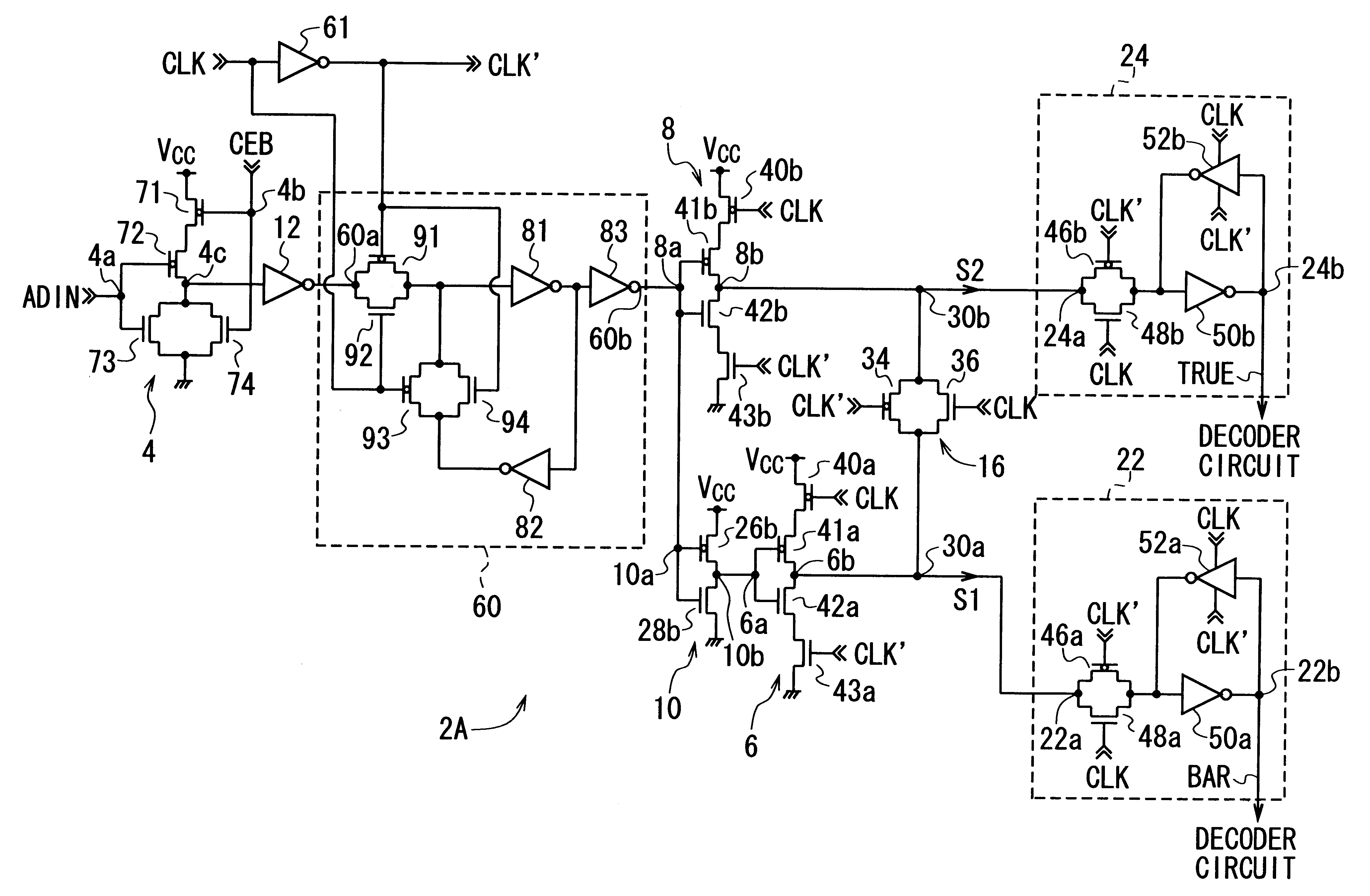
FIG. 6 shows an address buffer circuit 2A according a second embodiment of the present invention, which is comprised of an input stage 4, a first inverter circuit 6, a second inverter circuit 8, a third inverter circuit 10, a fourth inverter circuit 12, a first latch circuit 22, a second latch circuit 24, and a third latch circuit 60. This configuration is the same as that of the circuit 2 according to the first embodiment except that the fifth inverter circuit 14 is omitted, that the third latch circuit 60 and the inverter circuit 61 are added, and that the clock signal CLK is used as the control signals instead of the data latch signal DTL.
The input stage 4, the first, second, third and fourth inverter circuits 6, 8, 10, and 12, and the first and second latch circuits 22 and 24 in the address buffer circuit 2A are the same in configuration and operation as those in the circuit 2 according to the first embodiment of FIG. 3. Therefore, the explanation about these circuits is omitted...
PUM
 Abstract
Description
Claims
Application Information
 - R&D
- Intellectual Property
- Life Sciences
- Materials
- Tech Scout
- Unparalleled Data Quality
- Higher Quality Content
- 60% Fewer Hallucinations
Browse by: Latest US Patents, China's latest patents, Technical Efficacy Thesaurus, Application Domain, Technology Topic, Popular Technical Reports.
© 2025 PatSnap. All rights reserved.Legal|Privacy policy|Modern Slavery Act Transparency Statement|Sitemap|About US| Contact US: help@patsnap.com