

Power saving method using interleaved programmable gain amplifier and A/D converters for digital imaging devices
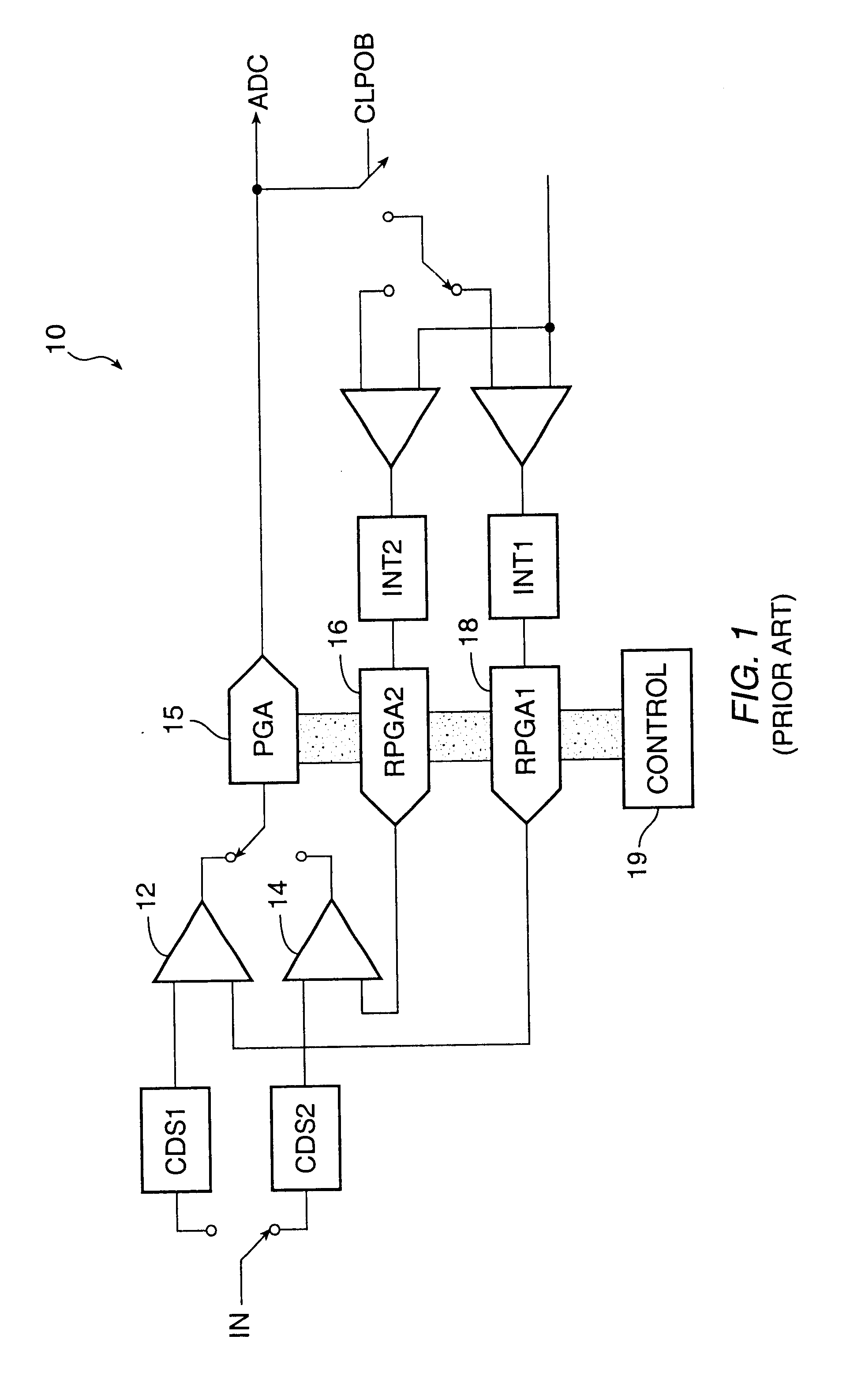
a power saving method and programmable gain technology, applied in the field of digital camera technology, can solve the problems of limiting the accuracy of the foregoing design to about 8 bits, introducing undesirable noise patterns, and limiting the gain to be no more than about 8 to 9 bits
- Summary
- Abstract
- Description
- Claims
- Application Information
AI Technical Summary
Problems solved by technology
Method used
Image

Examples
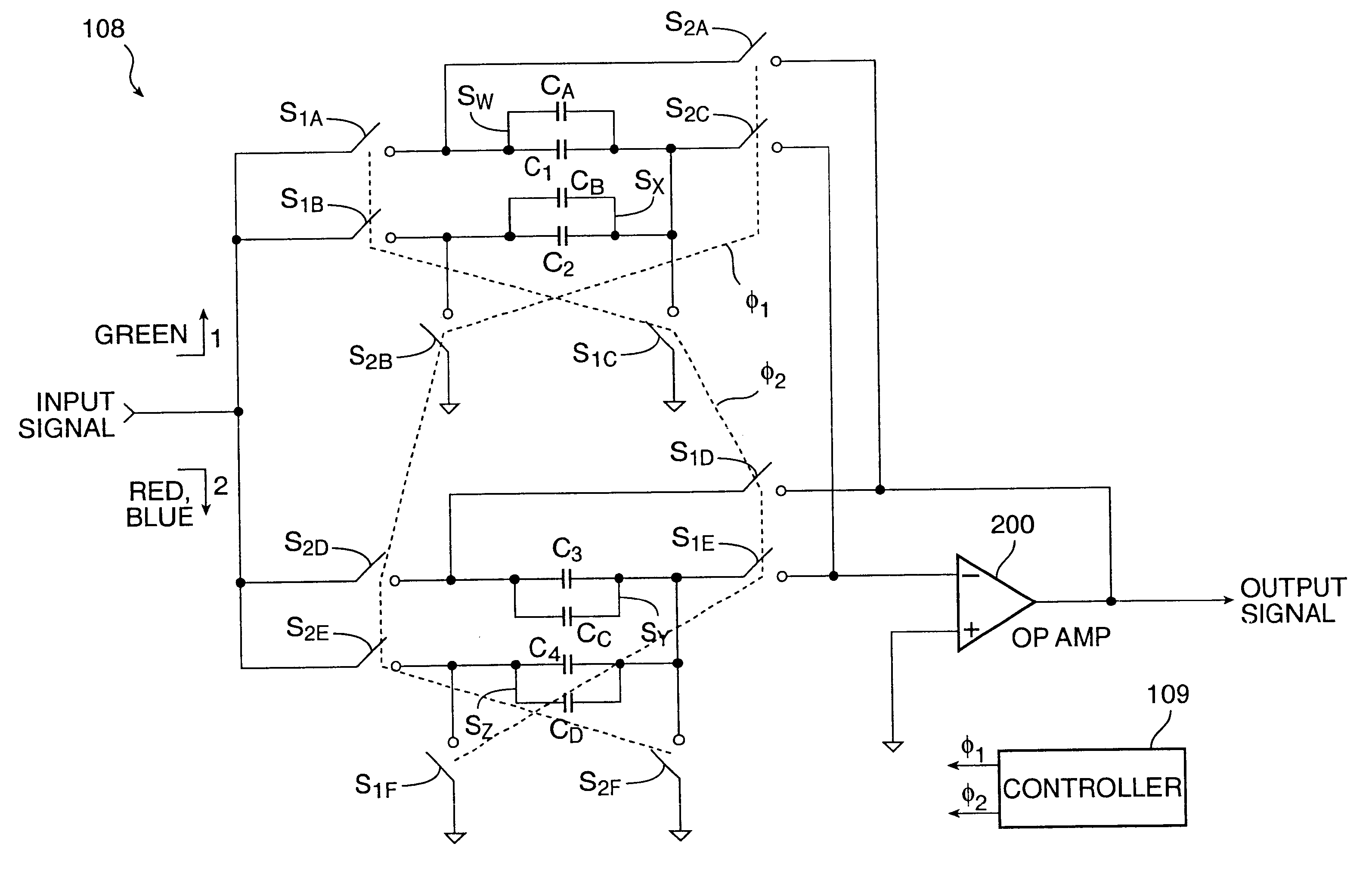
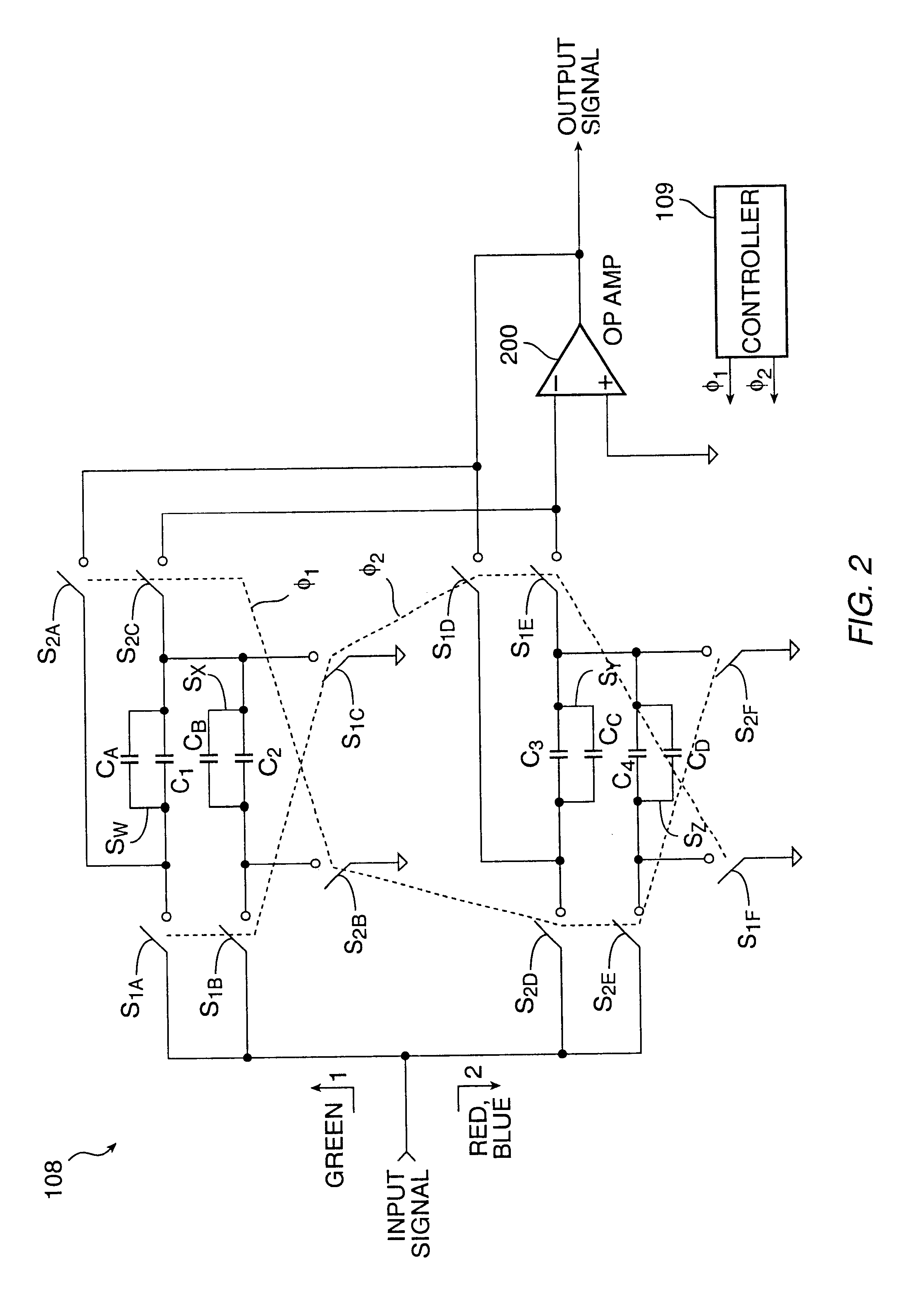
embodiment 108
A parallel signal path embodiment 108 is shown in FIG. 2 wherein two sets of capacitors (C1, C2); (C3, C4) are used during alternating phases of the controlling clock signals .O slashed.1, .O slashed.2 from a controller 109. The roles of the capacitors C1, C2, C3, C4 are changed every other clock cycle so that the two sets of capacitors share the operational amplifier 200 such that it is used for the entire clock cycle. During a first non-overlapping phase of two phase clocks, the switches S1A, S1B and S1C are closed and the input signal is sampled onto capacitors C1 and C2. During the second phase of the clock, which is likewise non-overlapping with the first phase, capacitor C1 is connected to the output (in the feedback loop) through switch S2A. The capacitor C2 is simultaneously connected to signal ground through switch S2B and the common node of the capacitors is connected to the input of the operational amplifier 200 through switch S2C. The paths alternate with non-overlapping...
embodiment 1100
FIG. 6 illustrates a further embodiment 1100 wherein the RED, GREEN and BLUE inputs are not time multiplexed on a single line but which are provided from three separate sources. This embodiment 1100 is suitable for implementation of a multiplexing / gain stage in a system illustrated in FIG. 7. Therein three CDS devices 121 carry respective R, G and B signals; one path is fed straight through to the element 1100. The other two devices 121 feed respective sample and hold circuits 123 which introduce phase delay to allow the element 1100 to respond to each of the signals serially. The output is fed to a PGA 140 according to the embodiment of FIG. 2, and to an ADC of the embodiment of FIG. 2.
Circuitry according to the invention can reduce power by a factor of two compared to conventional technology, which is a particularly valuable advance for battery-powered portable devices.
PUM
 Abstract
Description
Claims
Application Information