Overvoltage protection circuit with overvoltage removal sensing

a protection circuit and overvoltage detection technology, applied in the field of output circuitry, can solve problems such as undesirable current passing from the bus, 0v may experience a significant overvoltage event, and active devices may not be powered at equivalent potentials

Inactive Publication Date: 2002-02-05
SEMICON COMPONENTS IND LLC
View PDF5 Cites 24 Cited by
  • Summary
  • Abstract
  • Description
  • Claims
  • Application Information

AI Technical Summary

Benefits of technology

When the signal potential at OUT exceeds the potential of V.sub.cc by at least the threshold potential of a MOS transistor, transistor M3 remains off, transistor M5 turns on, and so transistors M4 and M6 also turn on. As a result, the potential at node A drops to that of GND. A logic HIGH is then imparted through inverter IV1 and logic gate 100 to the gate of M1, turning that pull up transistor off and thereby blocking current from OUT to V.sub.cc. When the overvoltage condition at OUT is removed, transistor M5 immediately turns off and the potential associated with node A immediately jumps up to V.sub.cc less the potential across R1. The signal passed to the gate of M1 effects a turn on of that transistor shortly thereafter and normal operating conditions of the output circuit 10 resume much faster than when using prior overvoltage protection devices. Importantly, it ensures that a logic HIGH to be transmitted by the output circuit 10 is maintained when coming out of the ove

Problems solved by technology

Increasingly, the active devices may not be powered at equivalent potentials.
For example, a PMOS transistor powered by a 3.3-volt supply and having an output coupled to a common bus that also has coupled to it an active device powered at 5.0V may experience a significant overvoltage event.
The result is an undesirable current passing from the bus to the power supply of the pullup transistor.
Further, a significant overvoltage condition at the pullup transistor's drain can create an unexpected turning on of that transistor when it is expected to be off.
Unfortunately, the Martin and other overvoltage protect

Method used


Image

  • Overvoltage protection circuit with overvoltage removal sensing
  • Overvoltage protection circuit with overvoltage removal sensing
  • Overvoltage protection circuit with overvoltage removal sensing

Examples


Embodiment Construction

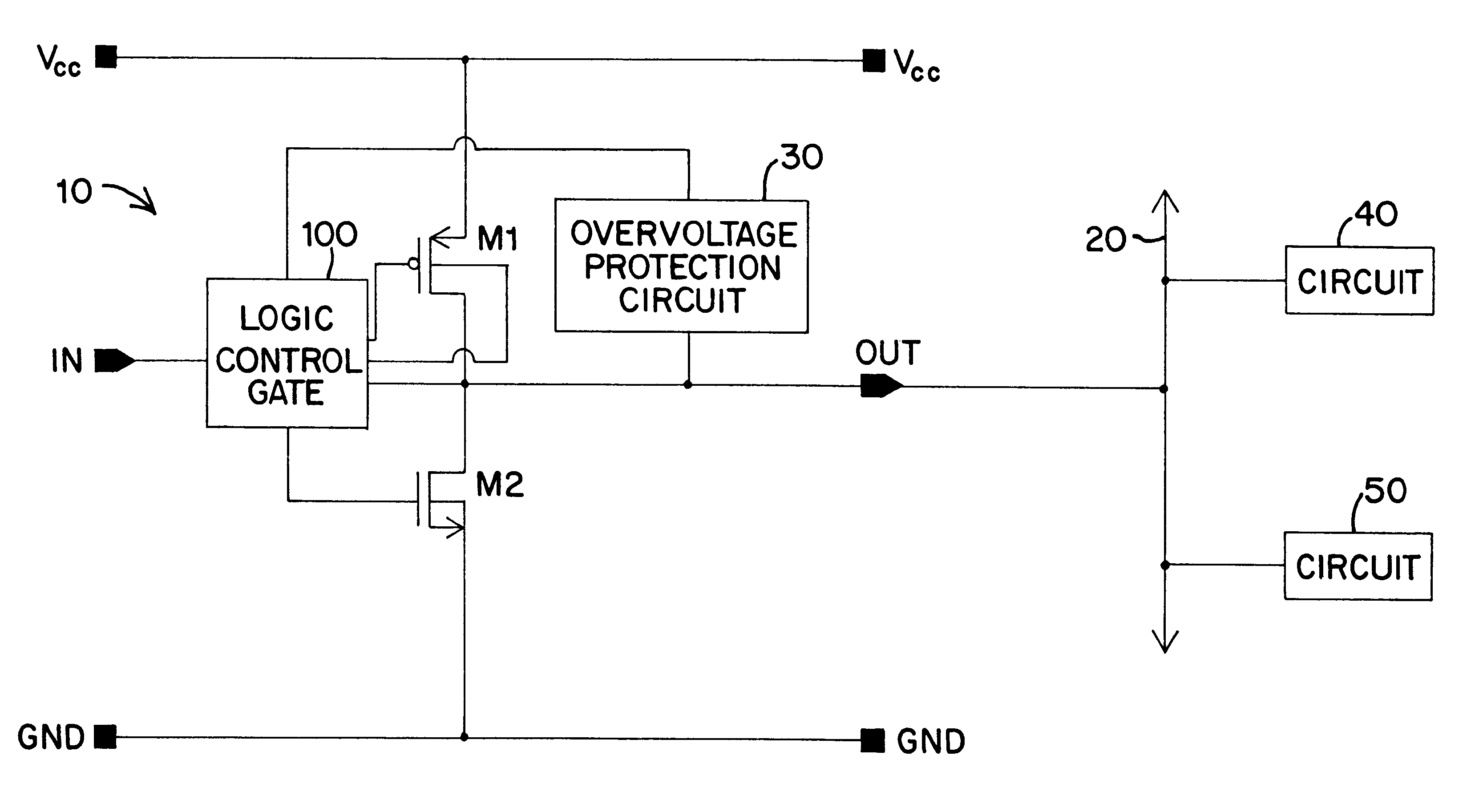
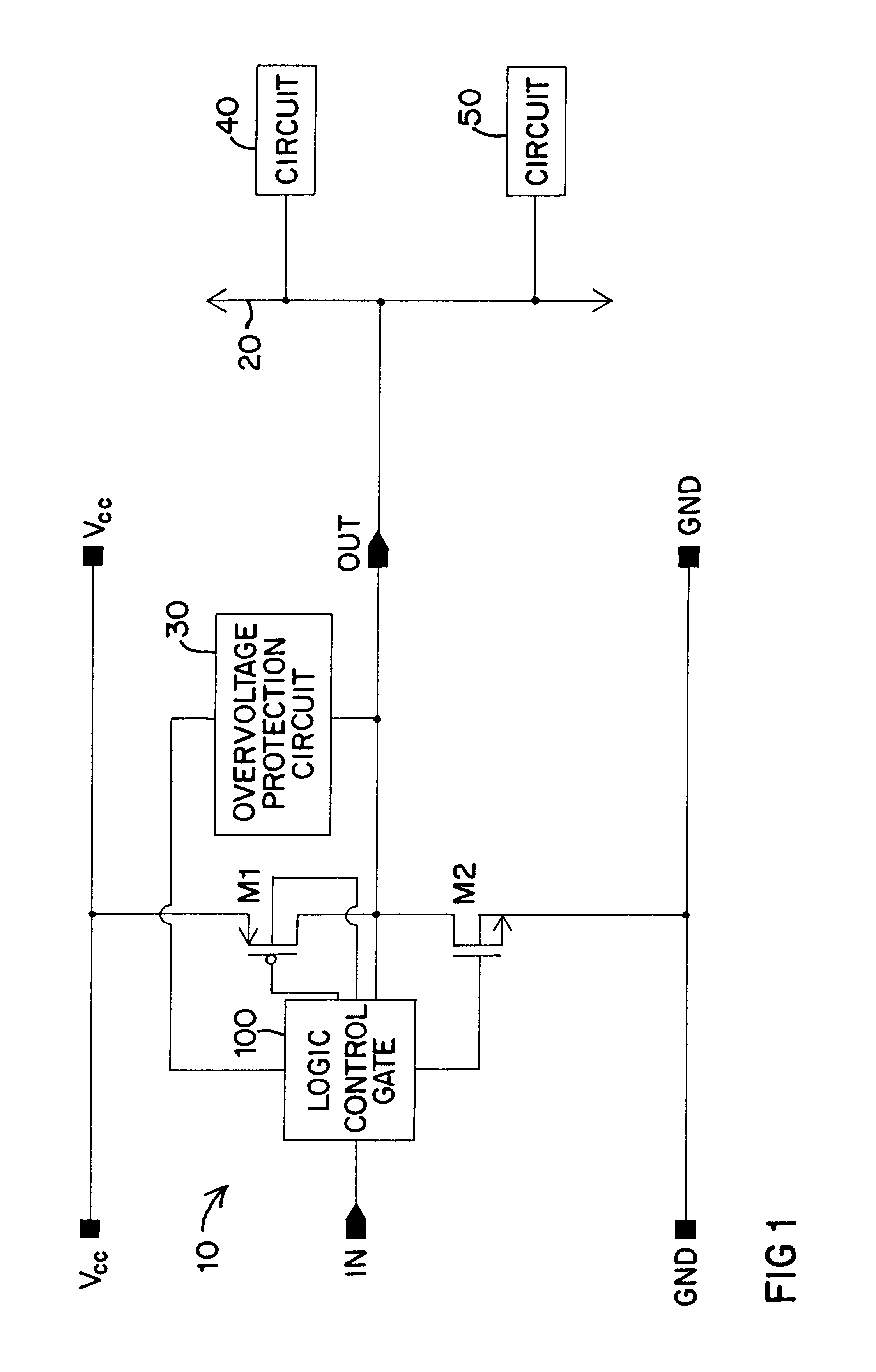
An output circuit 10 having pull up PMOS transistor M1 and pull down NMOS transistor M2 is shown in FIG. 1 coupled to a common bus 20. The output circuit 10 includes an input node IN for receiving an electrical signal to be transmitted to the bus 20 via output node OUT. Transistor M1 has a gate coupled through a control logic gate 100 to IN, a source coupled to high-potential power rail V.sub.cc, a drain coupled to OUT, and a bulk region also coupled to the control gate 100. Transistor M2 has a gate also coupled to IN through control gate 100, a source coupled to low-potential power rail GND, and a drain coupled to OUT. The circuit 20 further includes overvoltage protection circuit 30 coupled through the logic gate 100 to the gate of M1 and the output node OUT. Although the output circuit 10 is shown in FIG. 1 as a MOS-based output device, it is to be understood that the protection circuit 30 of the present invention may be used with bipolar and mixed MOS-bipolar output circuits tha...


PUM


Abstract

An overvoltage protection circuit arranged to sense removal of the overvoltage condition. The protection circuit blocks current passing through a pull up transistor of an output circuit to a high-potential supply rail during an overvoltage condition applied at a common bus. The protection circuit includes one protection branch controlled by the potential at the bus and powered by the high-potential supply rail of the output circuit to be protected. The protection circuit also includes a second protection branch controlled by the high-potential supply rail and powered by the potential on the bus. When an overvoltage condition occurs, the second branch is activated and regulates an output from the first protection branch. That output signal controls the control node of the pull up transistor of the output circuit to be protected. The two protection branches are configured such that removal of the overvoltage condition causes a rapid changing of the state of the output of the first protection branch so that the operating condition of the pull up transistor remains the same as it was prior to the overvoltage condition.

Description

1. Field of the Invention.The present invention relates to output circuitry having active overvoltage protection. More particularly, the present invention relates to circuitry having an output coupled to a common bus which bus may experience signal potentials exceeding the signal potential associated with the output circuitry. The present invention is an output control circuit having overvoltage protection and means for detecting an overvoltage condition as well as the removal of an overvoltage condition on the common bus and ensuring that the output signal of the output circuitry is maintained through the transition from the overvoltage condition.2. Description of the Prior Art.Electrical signal transmission circuits are used to transfer electrical signals of desired amplitude and strength. Signals are transferred from one sub-system to another by way of interfaces, i.e., buses, that couple active devices together. Increasingly, the active devices may not be powered at equivalent p...

Claims


Application Information

Patent Timeline
IPC IPC(8): H03K19/003H02H3/20H02H9/02H03K17/08H03K17/687
CPCH03K19/00315
Inventor MORRILL, DAVID P.
Owner SEMICON COMPONENTS IND LLC
Why Eureka
Try Eureka