Interconnect structure with gas dielectric compatible with unlanded vias

a dielectric and interconnecting structure technology, applied in the direction of basic electric elements, electric apparatus, semiconductor/solid-state device manufacturing, etc., can solve the problems of increasing energy consumption, slow data transmission rate, and undesirable capacitance and inductive coupling of wire lines

Inactive Publication Date: 2002-02-26
UNITED MICROELECTRONICS CORP
View PDF4 Cites 61 Cited by
  • Summary
  • Abstract
  • Description
  • Claims
  • Application Information

AI Technical Summary

Problems solved by technology

Closely spaced, parallel wiring lines can provide undesirable levels of capacitive and inductive coupling between adjacent wiring lines, particularly for higher data transmission rates through the arrays of parallel wiring lines.
Such capacitive and inductive coupling slow data transmission rates and increase energy consumption in a manner that can limit the performance of the integrated circuits.
For some aggressive circuit designs, the delays and energy consumption associated with the circuit's interconnect structure are a significant limitation on the circuit's performance.
The complexity of modem interconnect structures has become a major cost component for integrated circuit designs.
Various factors threaten to further increase the proportional expense of the interconnect structure within integrated circuits.
Adoption of these alternate dielectric materials has not been completely satisfactory to this point in time, due to the increased cost and processing difficulty associated with these alternative materials.
There are, however, aspects of the process described above for forming the FIG. 1 structure which are incompatible with certain manufacturing processes.

Method used


Image

  • Interconnect structure with gas dielectric compatible with unlanded vias
  • Interconnect structure with gas dielectric compatible with unlanded vias
  • Interconnect structure with gas dielectric compatible with unlanded vias

Examples


Embodiment Construction

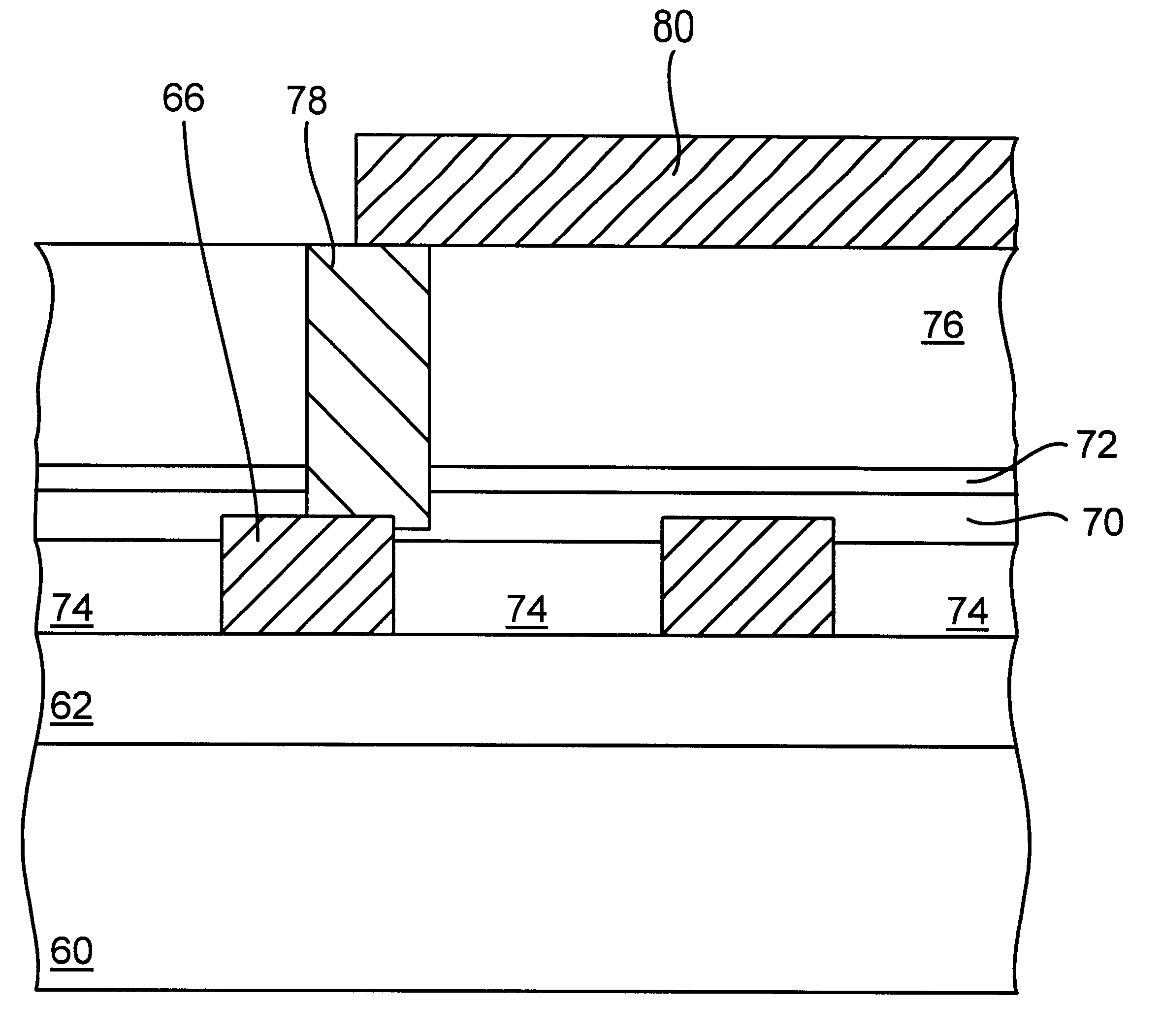
According to one aspect, the present invention forms an integrated circuit device by providing a pattern of wiring lines over an insulating layer, a first wiring line laterally separated from a second wiring line by a layer of sacrificial material. A portion of the layer of sacrificial material is removed to recess an upper surface of the layer of sacrificial material below upper surfaces of the first and second wiring lines. A layer of capping material is provided over the first and second wiring lines and over the recessed upper surface of the layer of sacrificial material. Then, a consumption reaction is performed through the layer of capping material to consume at least a further portion of the layer of sacrificial material, leaving an air dielectric between the first and second wiring lines bounded on an upper surface by the capping layer.

According to another aspect, the present invention forms an integrated circuit device by providing a pattern of wiring lines over an insulati...


PUM


Abstract

A multilevel interconnect structure is formed which uses air as a dielectric between wiring lines and which is compatible with the presence of unlanded vias in the interconnect structure. A layer of carbon is deposited over an insulating surface and then a pattern for trenches is formed in the surface of the layer of carbon. Metal is deposited in the trenches and over the layer of carbon and then a chemical mechanical polishing process is used to define wiring lines. An ashing or etch back process is performed on the carbon layer to recess its surface below the surfaces of the wiring lines. An oxide capping layer is provided over the recessed surface of the carbon and the wiring lines, for example using HSQ and curing, and then the carbon layer is consumed through the capping layer using an oxidation process. Air replaces the sacrificial carbon layer during the consumption reaction. Next, a silicon nitride etch stop layer is provided over the surface of the capping layer and then an intermetal dielectric layer is provided. A via is formed by etching through the intermetal dielectric, stopping on the etch stop layer, and then etching through the etch stop layer and the capping layer in distinct processes. The via is filled with a metal plug and then second level wiring lines are formed.

Description

1. Field of the InventionThe present invention relates to the formation of integrated circuit devices of the type that include multilevel interconnect structures.2. Description of the Related ArtModem integrated circuits include devices such as field effect transistors (FETs) or bipolar devices formed in and on a semiconductor substrate in combination with a multilevel interconnect structure formed above and in contact with the devices. The multilevel interconnect structure provides connections to and between different ones of the devices formed in the substrate and so is an increasingly important aspect of aggressive designs for integrated circuits. In many integrated circuits, the multilevel interconnect structure includes one or more arrays of wiring lines extending in parallel to provide connections to and between the devices in closely packed arrays of devices. Such arrays of devices are typical of integrated circuit memories and other aggressive circuit designs. Closely spaced...

Claims


Application Information

Patent Timeline
Patent Type & Authority Patents(United States)
IPC IPC(8): H01L21/70H01L21/768
CPCH01L21/7682H01L21/76802
Inventor SUN, SHIH-WEI
Owner UNITED MICROELECTRONICS CORP
Why Eureka
Try Eureka