Method and apparatus for wiring, wire, and integrated circuit

a technology of integrated circuits and wires, applied in the direction of solid-state devices, coatings, chemical vapor deposition coatings, etc., can solve the problems of increasing interconnection resistance, difficulty in sufficiently plugging the wiring material, and conventional plugging methods not working sufficiently

Inactive Publication Date: 2002-03-12
FUJITSU SEMICON LTD
View PDF14 Cites 12 Cited by
  • Summary
  • Abstract
  • Description
  • Claims
  • Application Information

AI Technical Summary

Problems solved by technology

There is a problem that it is difficult to plug the wiring material sufficiently into the via hole having a large aspect ratio using the conventional PVD method or CVD method. FIG. 7 shows a void formation generated by insufficient deposition method.
However, the conventional plugging method does not work sufficiently, which causes to generate a void 102.
This may further cause a problem to increase interconnect resistance or in a worse case, to generate disconnection.
The problem is brought by poor stepcoverage, i.e., a metal film is made nonuniformly on the side surface of the via hole 10 at an initial stage of deposition.
However, when the wetting layer having good wettability is formed nonuniformly on the side surface of the via hole 10, it is difficult to plug the wiring material sufficiently.
This is because the PVD method cannot plug the wiring material sufficiently because of geometric reason.
Therefore, the wiring material cannot be plugged sufficiently.
As has been described, it is impossible to plug the wiring material sufficiently using the conventional plugging method.
Therefore, there is a problem to generate a void, which causes to increase interconnect resistance, and in a worse case, to generate disconnection.
The relaxation can progress at room temperature, however, it takes a large amount of time to relax at room temperature.
When the precursors is contacted with the surface of the via hole, an electron is supplied from the electron donative layer, which causes disproportionation.

Method used


Image

  • Method and apparatus for wiring, wire, and integrated circuit
  • Method and apparatus for wiring, wire, and integrated circuit
  • Method and apparatus for wiring, wire, and integrated circuit

Examples


Embodiment Construction

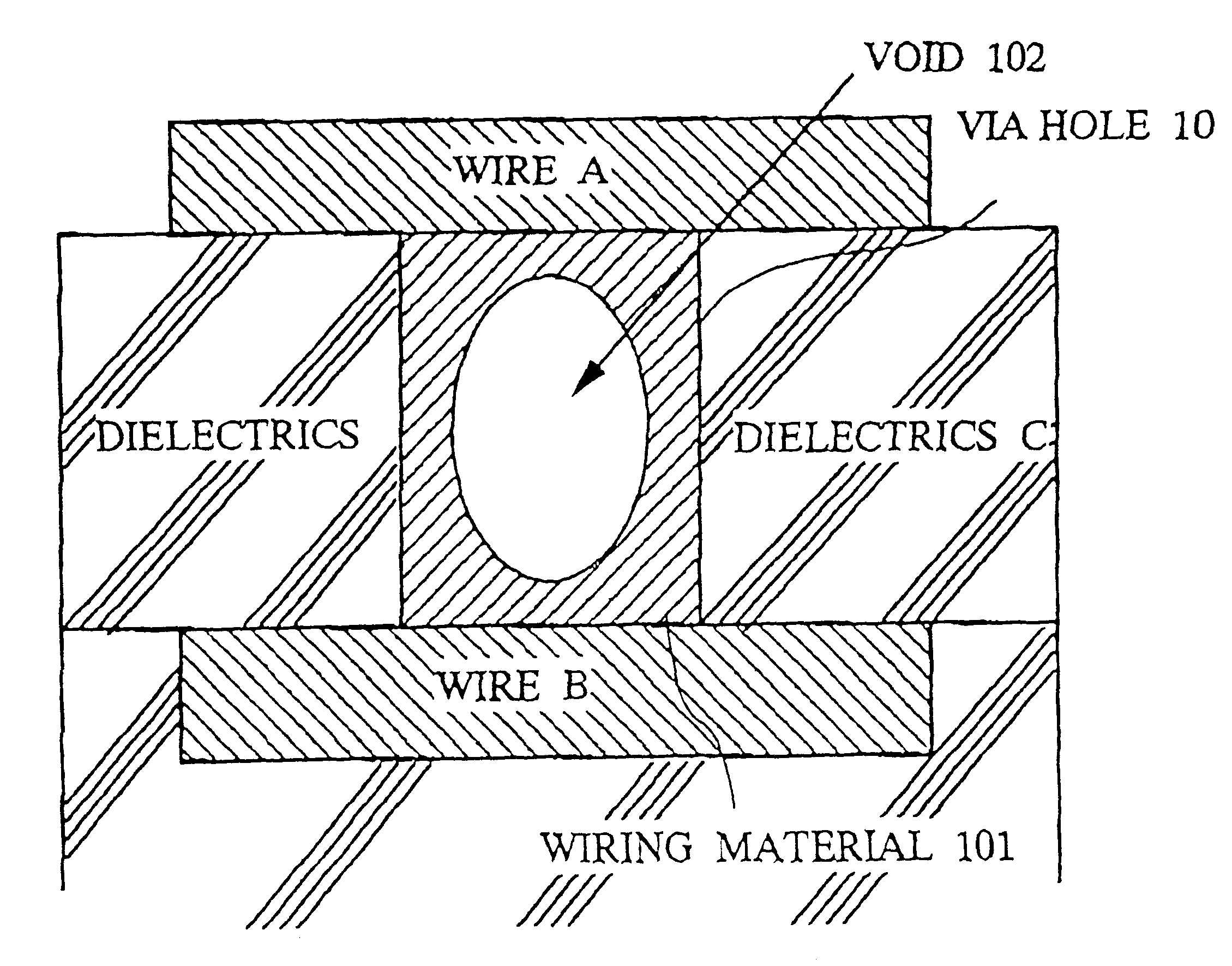
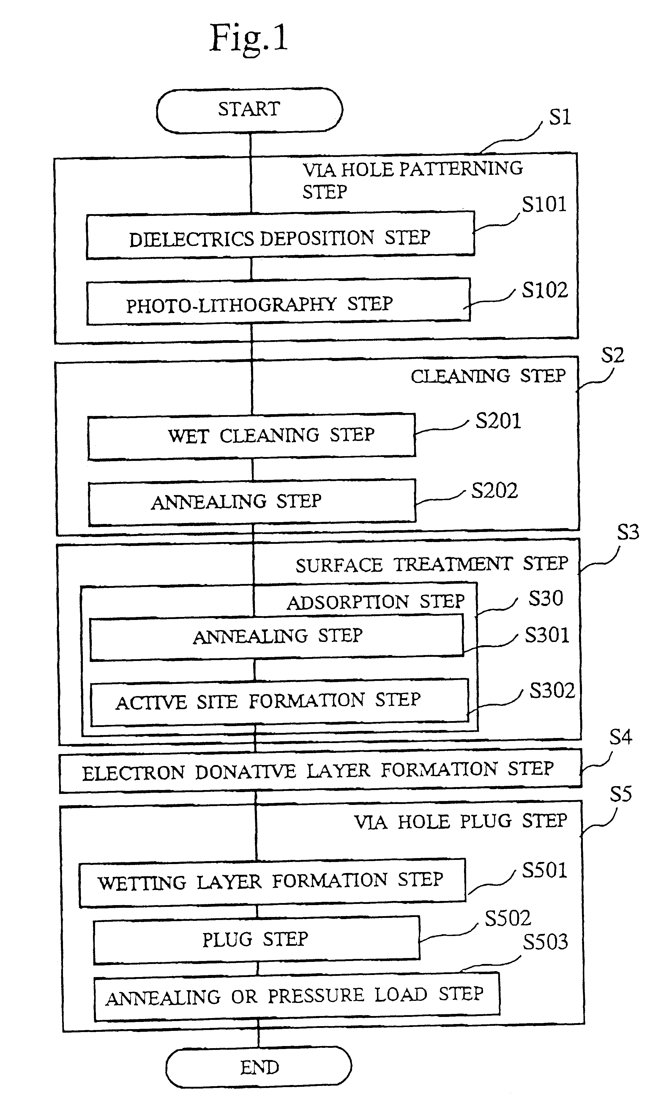
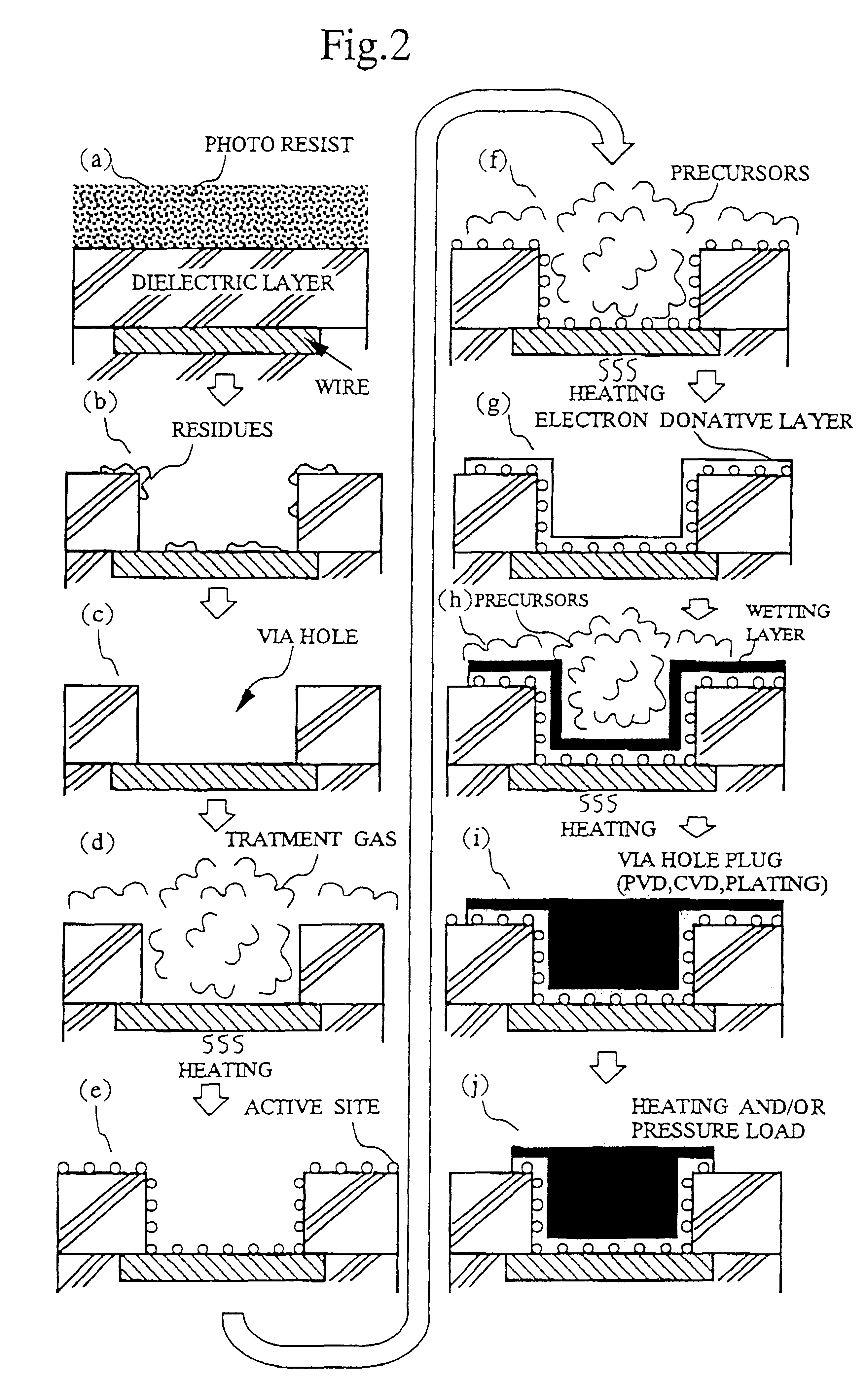
In the following, an example case that the embodiment of the invention is applied to plugging Cu (copper) or Al (aluminum) will be explained. As shown in FIG. 4, an apparatus for wiring according to the present invention has a surface treatment unit 1, an electron donative layer forming unit 2, and a plug unit 3. Each unit can control heating and pressuring.

Arrows in FIG. 4 show the path for carrying a wafer to make a wire thereon. The wafer provided with a via hole in an interlayer dielectric film produced on the wafer, and the wafer is carried out from "OUT".

The wafer provided with the via hole in the interlayer dielectric film and annealed is carried in the surface treatment unit 1 shown in FIG. 4. The surface treatment unit 1 heats the wafer up to 400.degree. C. from the room temperature, and supplies hydrazine (N.sub.2 H.sub.4) to the surface of the wafer as shown in FIG. 5. Then, when the hydrazine is contacted with the surface of the via hole, covalent band between nitrogen a...


PUM

PropertyMeasurementUnit
aspect ratioaaaaaaaaaa
temperatureaaaaaaaaaa

Abstract

The present invention provides a method for wiring, which plugs conductive material sufficiently into a via hole produced in dielectronics (hereinafter, referred to as "a via hole") and prevents generating a void. The via hole is made through a via hole patterning step and a cleaning step. At a surface treatment step, substance having chemical affinity (active site) is adsorbed to the surface of the via hole. Next, an electron donative layer is made by depositing substance having an electron donative characteristic on the active sites acting as cores at an electron donative layer formation step. Then, the wiring material is plugged at a via hole plug step.

Description

1. Field of the InventionThe present invention relates to a method and an apparatus for wiring, a wire and an integrated circuit. In particular, the invention relates to, for example, a method and an apparatus for wiring whose material is plugged sufficiently so as to prevent generation of a void or to prevent disconnection, a wire and an integrated circuit having the wire.2. Description of the Related ArtRecently, semiconductor devices have been integrated so highly that a designing rule of nanometer level has been applied to a design of integrated semiconductor devices instead of the designing rule of micron level (e.g., The National Technology Roadmap for Semiconductors Technology Needs, SIA, 1997 edition). A multi-layered wiring structure including wires made on each layer of multiple layers has been utilized to integrate semiconductor devices. An electric interconnection among these wires made on the multiple layers inserting an interlayer dielectronics is connected by plugging...

Claims


Application Information

Patent Timeline
Patent Type & Authority Patents(United States)
IPC IPC(8): H01L21/02H01L21/70H01L21/285H01L21/768C23C16/02H01L21/28H01L21/77
CPCH01L21/28556H01L21/76802H01L21/76814H01L21/76838H01L21/76871H01L21/76876H01L21/76877H01L21/76843H01L2221/1089H01L21/77
Inventor OHBA, TAKAYUKI
Owner FUJITSU SEMICON LTD
Why Eureka
Try Eureka