Structure and method for reduction of power consumption in integrated circuit logic

a technology of integrated circuit logic and power consumption reduction, which is applied in the direction of logic circuits using specific components, logic circuit coupling/interface arrangement, pulse technique, etc., can solve the problem that the technique of reducing the operational voltage to reduce the power dissipation is approaching its physical limitations, and the operational voltage of an integrated circuit cannot be significantly reduced below 0.9 volts

Inactive Publication Date: 2002-04-23
TELOGY NETWORKS
View PDF3 Cites 15 Cited by
  • Summary
  • Abstract
  • Description
  • Claims
  • Application Information

AI Technical Summary

Problems solved by technology

The dissipation of power generates heat.
The technique of reducing the operational voltage to reduce power dissipation is approaching its physical limitations due to a variety of reasons, including the minimal necessary voltage for the logic elem

Method used


Image

  • Structure and method for reduction of power consumption in integrated circuit logic
  • Structure and method for reduction of power consumption in integrated circuit logic

Examples


Embodiment Construction

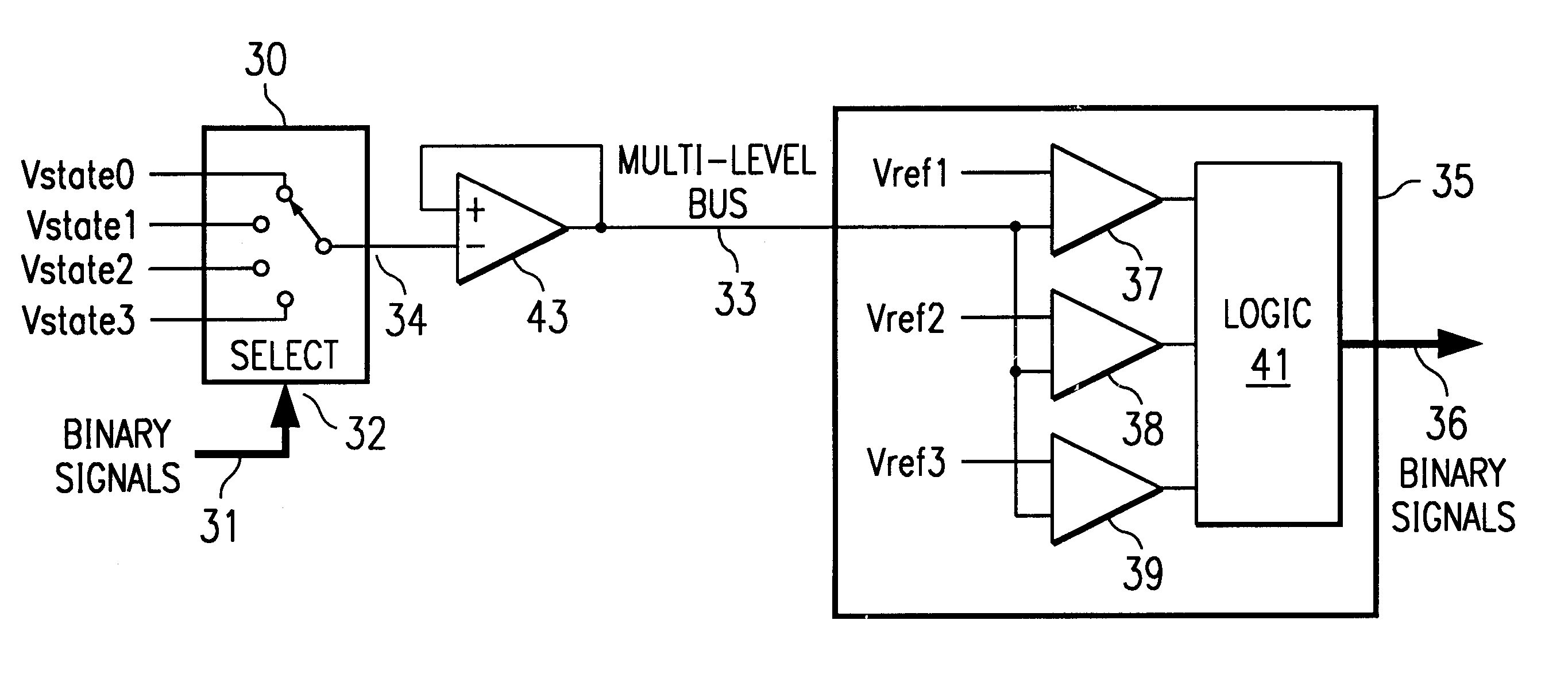
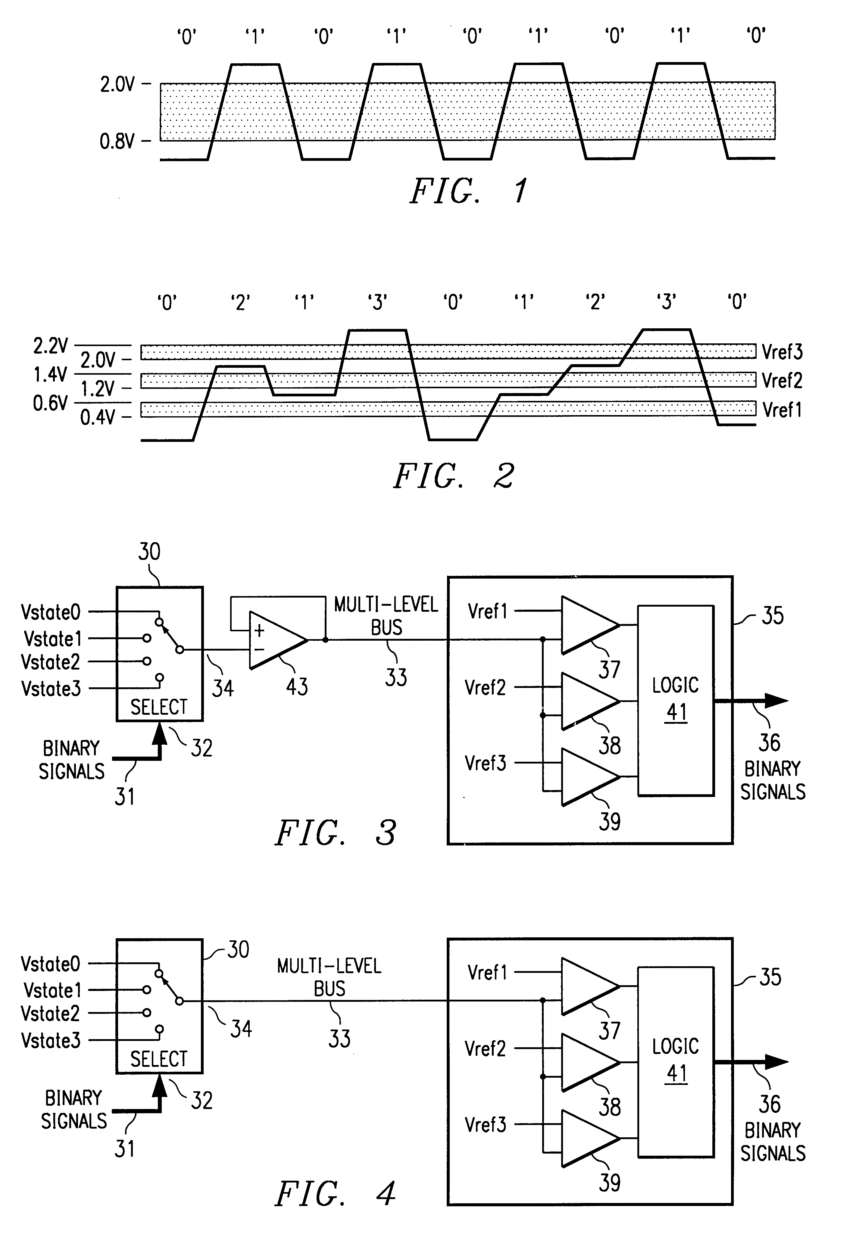
As illustrated in FIG. 1, a single signal line with a single threshold can have two states "0" and "1". The conductor line is either charged above 2.0 v or discharged below 0.8 v. When the line is above 2.0 v the logic state of the line is 1. When the voltage on the line is below 0.8 v, the logic state of the line is 0. The line dissipates power in watts based upon the voltage change of 1.6 v in charging or discharging between these two logic states (ie. 0.6 v to 2.2 v). A single line can therefore transmit two logic values. In order to transmit a logic representation of four separate values in binary code (00, 01, 10, 11), two single threshold lines are needed. These two lines, by switching logic states between "0" and "1" can represent binary numbers 00, 01, 10 and 11. Table I illustrates the transition between all possible logic states, and the voltage change relative to the power dissipation for each transition, given a pair of two state conductor lines as illustrated in FIG. 1:...


PUM


Abstract

A reduced power dissipation integrated circuit. Power dissipation within a CMOS circuit is reduced by substitution of multi-level buses with several thresholds for binary state buses with a single threshold. A significant portion of an IC's power dissipation is consumed by the act of charging and discharging data and address busses within the IC because theses busses possess the highest capacitances of any of the nodes within the part. The present invention uses a series of thresholds from a minimum voltage to a maximum voltage. Below the minimum threshold voltage Vref1, the logic state would be "0". Above the maximum threshold voltage Vrefn, the logic state would be "n". A series of defined thresholds, Vref1, Vref2, . . . Vrefn, between the minimum and maximum voltages define a series of logic states 0, 1, 2 . . . n+1 between 0 and n+1.

Description

1. Field of the InventionThe present invention relates to integrated circuit power dissipation. More specifically, the present invention relates to a lower power dissipation bus structure within an integrated circuit or a circuit board.2. Description of the Background ArtIntegrated circuits operate by charging and discharging internal components in order to switch between logic states. The frequency at which an integrated circuit switches between logic states is referred to as its switching frequency. Each switching cycle dissipates power in charging and discharging components and in passing the power through busses to and from the logical components. The faster the switching frequency, the greater the power dissipation in a given period of time.The dissipation of power generates heat. The quantity of heat generated in a given area of an integrated circuit is directly proportional to the density of the logic elements and circuitry on the integrated circuit chip. The heat generated s...

Claims


Application Information

Patent Timeline
IPC IPC(8): H03K19/00H04L25/49
CPCH04L25/4917H03K19/0002
Inventor KRASNANSKY, KEITH
Owner TELOGY NETWORKS
Why Eureka
Try Eureka