However, the foregoing vacuum filling method, which is used for the
cell employing the glass substrates, requires a long time for discharging the air from the
cell and for filling the liquid
crystal material thereinto, and therefore suffers from a problem of low productivity.
In particular, this problem becomes remarkable in the structure using large substrates.
Such a problem also arises that an unnecessary liquid crystal material adheres to the cell end surface, resulting in a large loss of the liquid crystal material.
Further, when producing a plurality of the liquid
crystal display element, a plurality of the inlet of the cell are brought into contact with the liquid crystal material in a reservoir, and thereby a plurality of cells are immersed several or many times in the liquid crystal material in the reservoir, and resulting in that the liquid crystal material in the reservoir is polluted.
In particular, this problem becomes remarkable when both of the substrates are the film substrates.
However, this method requires complicated operations for fixing the film substrate to the glass substrate, and removing it from the glass after filling the liquid crystal material.
Further, the film substrate may be damaged or deformed.
Problems other than the above may also arise.
In the above method of fixing the film substrate to the glass for manufacturing the liquid
crystal display element, increase in number of steps as well as complication thereof are unavoidable, and the larger size of the substrate makes the manufacturing more difficult.
However, these manners cannot yet sufficiently achieve the uniformity in gap between the substrates, and therefore the uniformity in thickness of the liquid crystal material.
However, provision of the large amount of spacer particles on the substrate increases the cost, and reduces the area of the display region, and thus the display performance reduces.
Further, an excessive pressure may destroy the spacer particles and / or the substrates.
In the case where the spacer particles are disposed in advance on the substrate before performing the substrate fixing step, the excessive pressure may move the spacer particles because each portion of the substrate are subjected to the pressure (e.g., by the movement of the pressing member relative to the substrate) in the substrate fixing step, and therefore the excessive pressure may cause irregularities in gap between the substrates.
If the substrate fixing speed (pressure
moving speed) is excessively large, the liquid crystal material cannot be spread uniformly over the whole space between the substrates, and an unfilled region is left.
An excessively high
heating temperature increases the
volume expansion of the liquid crystal material, and thereby a large volume shrinkage occurs when the temperature of the liquid crystal material lowers after fixing of the substrates, and therefore bubbling occurs.
If the substrate fixing speed (heating
moving speed) is small, a large amount of heat is supplied to the liquid crystal material, and therefore a large
volume expansion of the liquid crystal material will occur.
The fixing speed (heating
moving speed) likewise affects the transmission of heat to the resin structure, and thus affects the adhesivity.
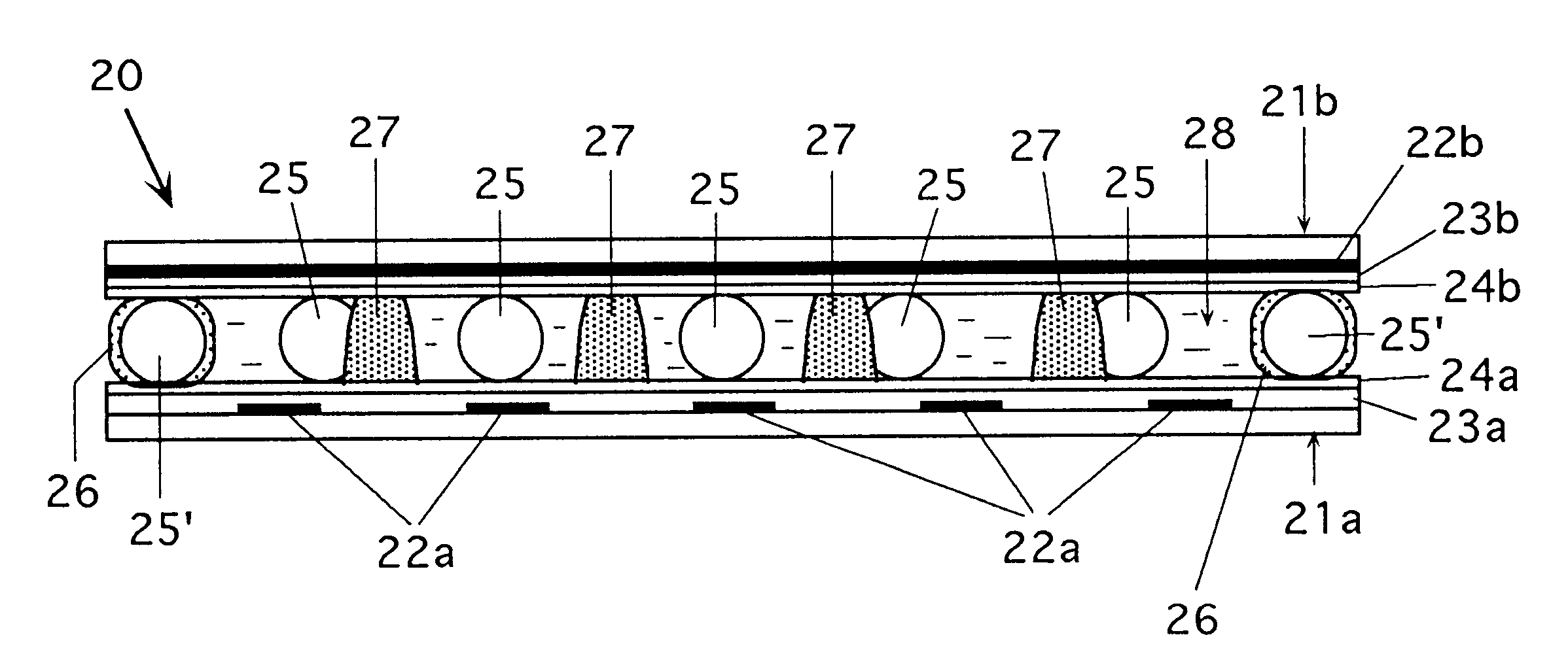
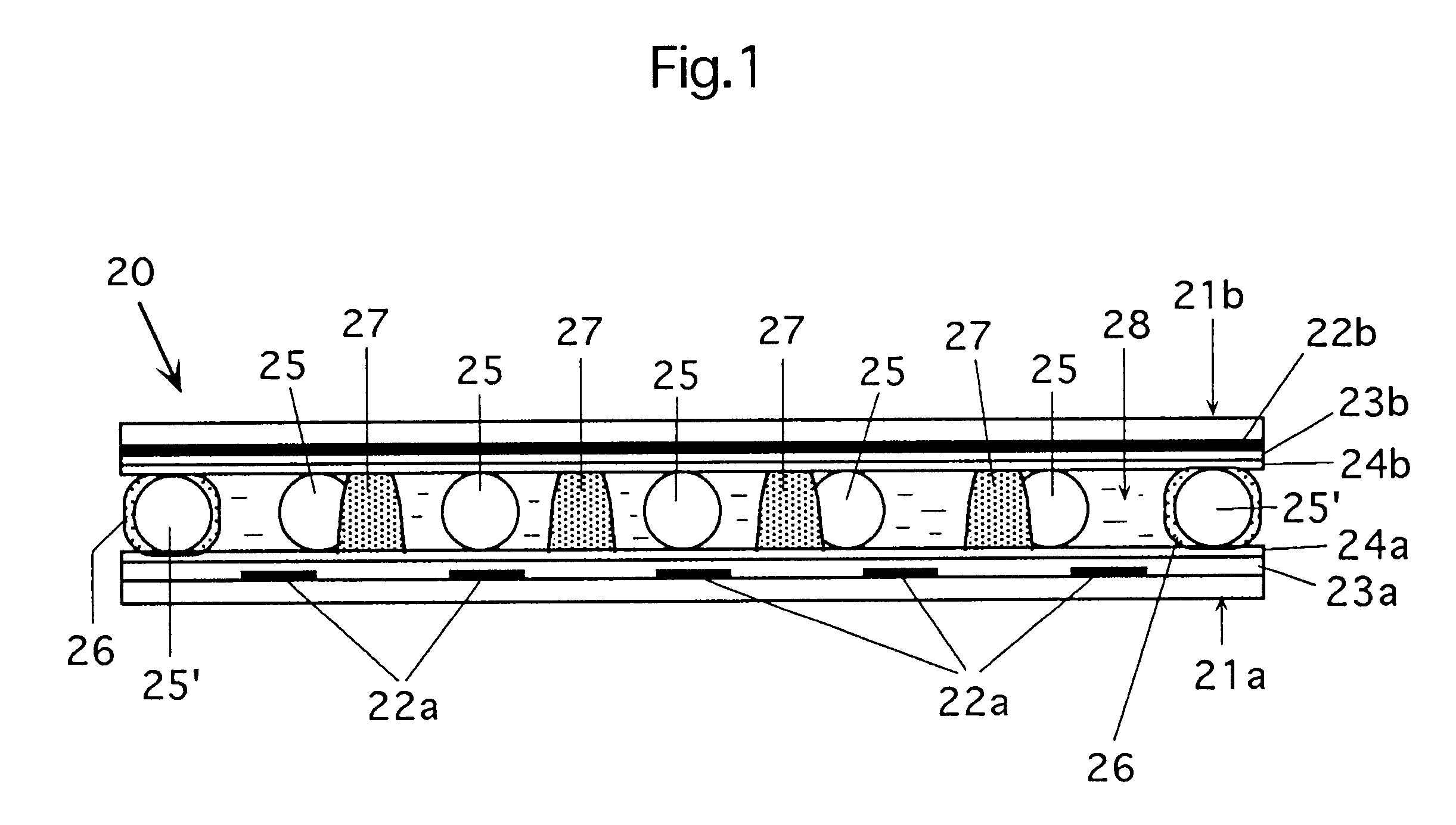
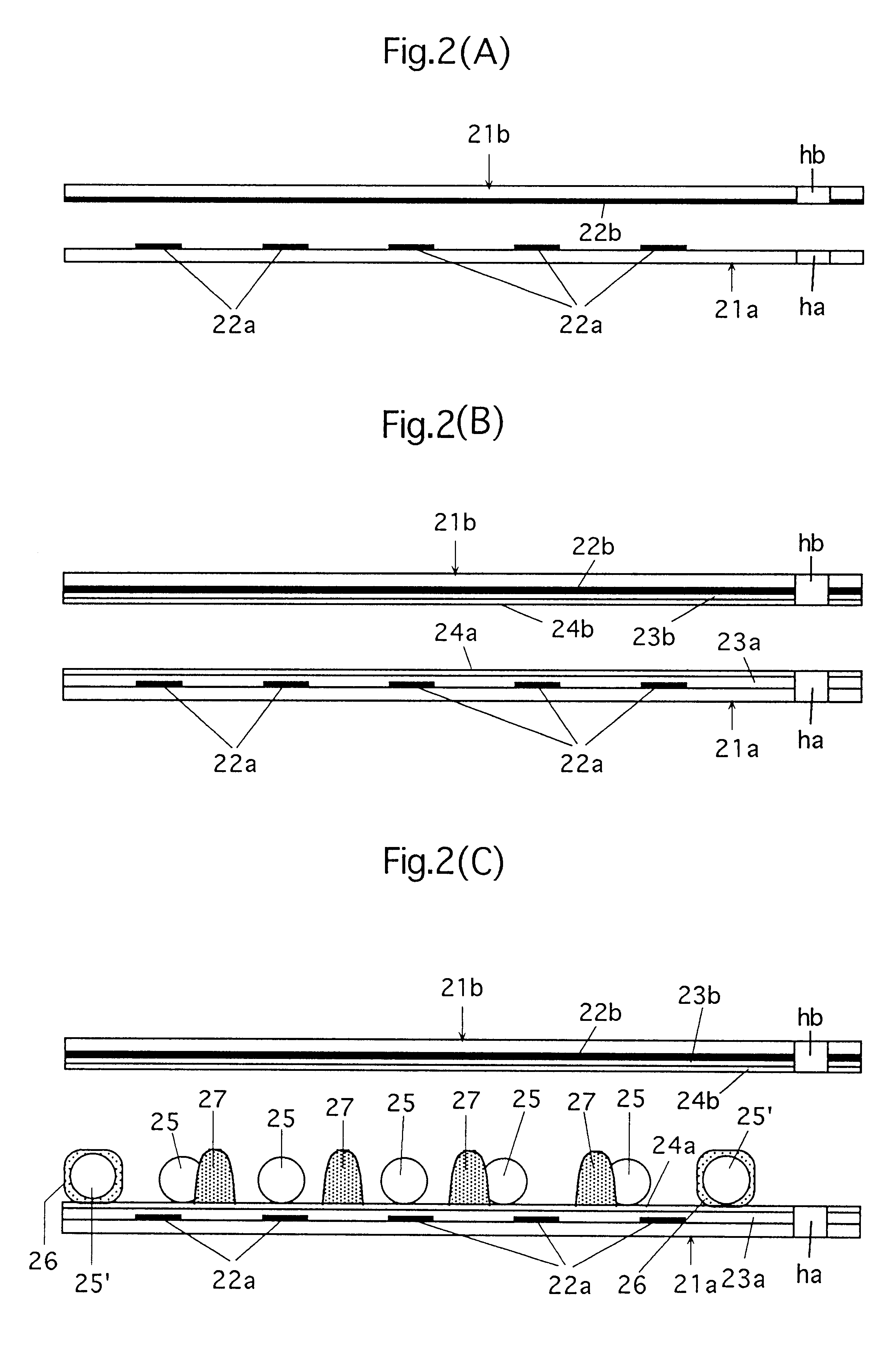
In the case where the heat is applied to the substrate during fixing, the substrates are bent due to the pressure and heat if the density of the spacer particles disposed between the substrates is excessively small.
As described above, when the substrates are bent due to the excessively small density of the spacer particles, the gap between the substrates excessively decreases.
When the volume shrinkage of the liquid crystal material occurs, e.g., due to lowering in temperature after completion of the liquid
crystal display element, further compression of the liquid crystal display element is unlikely to occur because the whole volume thereof is still small.
Therefore, bubbling is likely to occur in the display element.
If the impulse F is smaller than the above range, the pressure is insufficient so that irregularities occur in distance between the substrates.
If the impulse F exceeds the above range, the pressure is excessively large so that breakage of the spacer particles and / or the substrates as well as flow of the spacer particles may occur, resulting in irregularities in gap between the substrates.
If the parameter X is excessively small, failures occur in adhesion of the
adhesive material and the resin structures, if employed, to the substrates, resulting in a problem that the fixed substrate peels off.
An excessively large value of the parameter X is liable to cause disadvantages such as bubbling in the liquid crystal material.
When the volume shrinkage of the liquid crystal material occurs due to, e.g., lowering in temperature after production of the display element, the bubbling is liable to occur.

