High frequency MOSFET switch

a high-frequency mosfet switch and switch technology, applied in electronic switching, pulse automatic control, pulse technique, etc., can solve the problems of increasing the on-resistance of the transistor, significant difficulty in propagating signals, and inability to pass signals attenuated,

Inactive Publication Date: 2002-05-28
SEMICON COMPONENTS IND LLC
View PDF14 Cites 82 Cited by
  • Summary
  • Abstract
  • Description
  • Claims
  • Application Information

AI Technical Summary

Problems solved by technology

Nevertheless, it has been determined that most silicon MOS transistor switches configured in the manner shown in FIG. 1 have significant difficulty in propagating signals between A and B when such signals exceed transmission frequencies on the order of 400 MHz.
It may appear to be possible to improve this characteristic by reducing the size of M1; however, there is an undesirable trade-off involving an increase in the on-resistance of the transistor.
The dominating impedance at such frequencies causes an unacceptable attenuation of the signal to be passed.
As earlier noted, this cannot be resolved by reducing the gate size of M1 as that drives up the drain-source resistance undesirably.

Method used


Image

  • High frequency MOSFET switch
  • High frequency MOSFET switch
  • High frequency MOSFET switch

Examples


Embodiment Construction

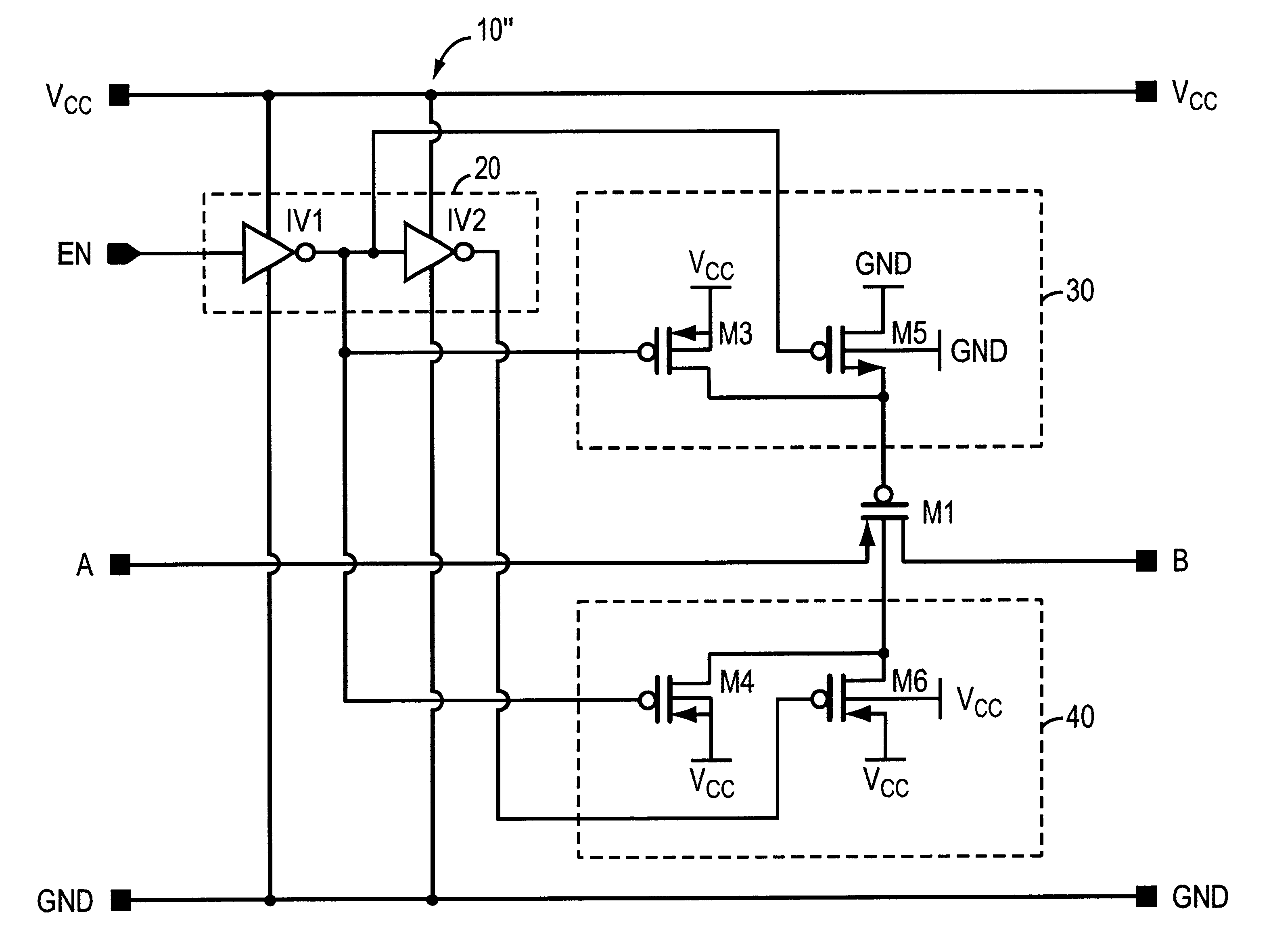
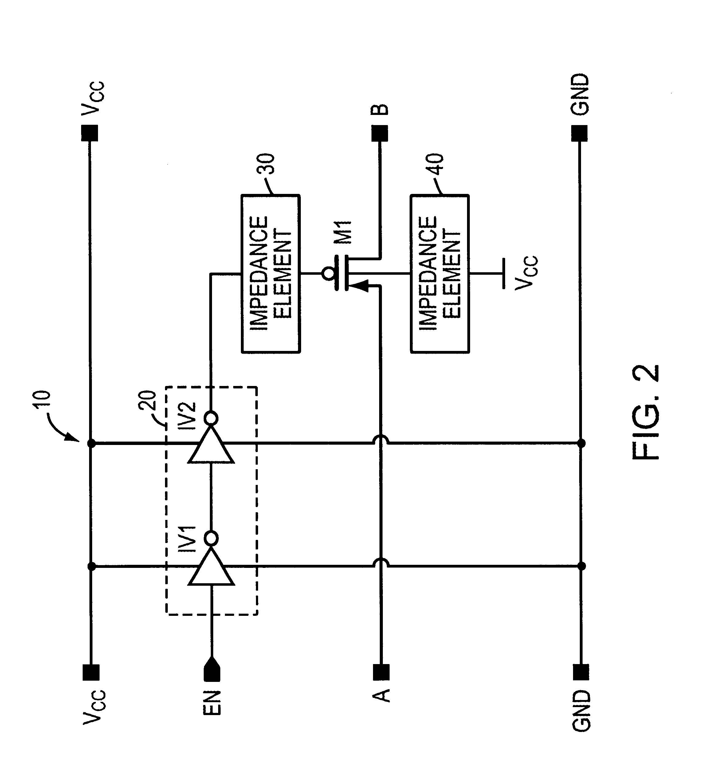
A high-frequency switch circuit 10 of the present invention is shown in FIG. 2. The circuit 10 includes an inverter stage 20 preferably formed of inverters IV1 and IV2 and PMOS pass gate transistor M1, much as in the prior-art switch shown in FIG. 1. Of course, the inverter stage 20 may be formed of a plurality of pairs of inverters, or some alternative form of enable signal propagation mechanism. The circuit 10 also includes a first impedance element 30 and a second impedance element 40, wherein element 30 is coupled between the output of inverter stage 20 and the gate of M1 and element 40 is coupled between the bulk of M1 and high-potential power rail Vcc. An enable signal coming from a control circuit (not shown) by output enable node EN is preferably coupled to the input of the inverter stage 20 to substantially define the control of the operation of transistor M1 by its gate. Inverters IV1 and IV2 are typically powered by high-potential rail Vcc and low-potential rail GND. It i...


PUM


Abstract

A high-frequency switch circuit having an MOS pass gate or transfer transistor. The switch circuit of the invention includes a first impedance element coupled to the gate of the transfer transistor and, preferably, an alternative second impedance element coupled to the bulk of the transfer transistor. One or both of the impedance elements substantially negates the low-parasitic shunt capacitance associated with the transfer transistor that controls signal attenuation under high frequency operation. The impedance element is coupled in series with that parasitic capacitance to increase substantially the impedance of that pathway, thereby increasing substantially the passable bandwidth. The impedance element may simply be a resistor. The switch circuit is suitable for use in an array of applications, including signal propagation in computing systems, routers, and flat panel screen displays.

Description

1. Field of the InventionThe present invention relates to electronic switches. In particular, the present invention relates to semiconductor switches, including those formed of one or more metal-oxide-semiconductor field effect transistors (MOSFET). More particularly, the present invention relates to semiconductor switches capable of switching at relatively high frequencies, including those frequencies above about one gigahertz.2. Description of the Prior ArtDevelopments in semiconductor technology have created the capability to produce low-cost, highly reliable switches that are, effectively, implementations of mechanical relays. They have been found to be of particular use, when implemented, as single pole, single throw, type relays, but are not limited thereto. Semiconductor switches are being used more and more as replacements for the prior mechanical relays, due to the high switching speed available as well as their ability to transfer relatively high currents without failure. ...

Claims


Application Information

Patent Timeline
Patent Type & Authority Patents(United States)
IPC IPC(8): H03K17/16H03K17/04H03K17/0412H03K17/687H01P1/15H03K17/00H03K17/06
CPCH03K17/04123H03K17/687H03K17/162H03K2217/0018H03K17/04
Inventor GOODELL, TRENOR F.
Owner SEMICON COMPONENTS IND LLC
Why Eureka
Try Eureka