Ball grid array package

a grid array and ball technology, applied in the direction of printed circuit manufacturing, printed circuit components, electrical apparatus construction details, etc., can solve the problems of poor reliability of the bonding between the solder ball and the solder ball, the routing density cannot increase, and the manufacturing cost will also increas

Inactive Publication Date: 2002-05-28
SILICONWARE PRECISION IND CO LTD
View PDF3 Cites 144 Cited by
  • Summary
  • Abstract
  • Description
  • Claims
  • Application Information

AI Technical Summary

Problems solved by technology

Consequently, the solder ball 118 and the center area 104' would separate from the surface 101 of the substrate 100 which would result in poor reliability on the bonding between the solder ball 118 and the substrate 100.
Consequently, the routing capability of the substrate 300 will...

Method used


Image

  • Ball grid array package
  • Ball grid array package
  • Ball grid array package

Examples


Embodiment Construction

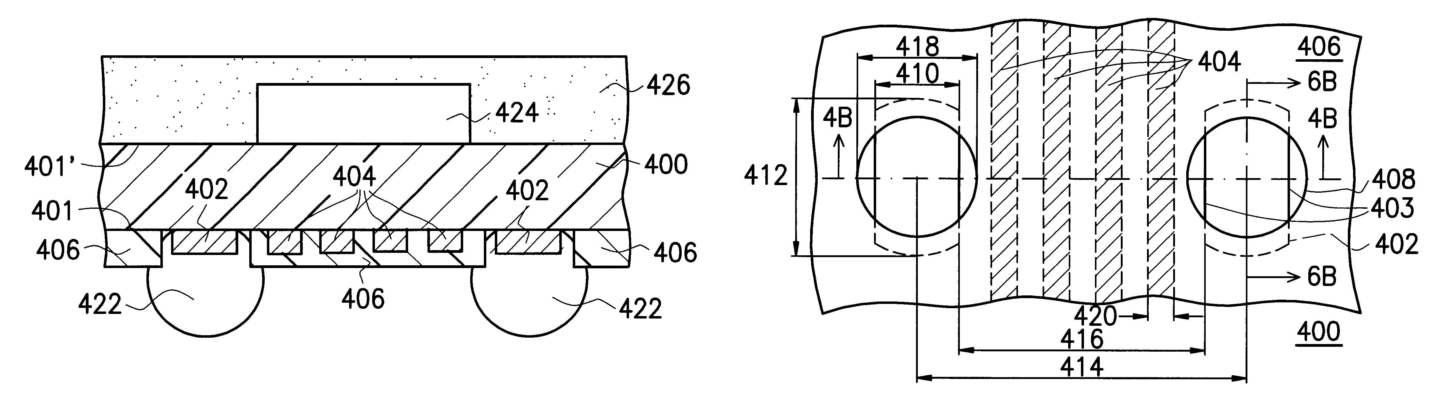
FIG. 4A to FIG. 4D are schematic cross-sectional views of a ball grid array package according to a preferred embodiment of the present invention. As shown in FIG. 4A, a plurality of ball pads 402 and conductive traces 404 first are formed on a surface 401 of a substrate 400 used as chip carrier, wherein the conductive traces 404 are disposed in between the adjacent ball pads 402. The substrate 400 can be made of prepreg of hard resin having high "glass transition temperature such as "Glass Epoxy Resin", "Bismaleimide-Triazine (BT)", etc., thereby forming FR-4 substrate, FR-5 substrate, and BT substrate, etc. The material used for the ball pads 42 and the conductive traces 404 can be made of electrically material such as copper.

Next, as shown in FIG. 4B, solder resist is coated on the first surface 401 having ball pads 402 and conductive traces 404 to form a solder mask 406 in order to cover all the conductive traces 404 and a portion of each of the ball pads 402. Ball pad openings 4...


PUM


Abstract

A ball grid array package comprises a substrate having a first surface and a second surface, a chip, an insulating material, and a solder ball. The surface of the substrate comprises ball pads, conducting traces, and solder masks wherein the conducting traces are disposed in between the adjacent ball pads, and are covered by the solder mask, in addition, a portion of each of the ball pads is also covered by the solder mask. The solder mask includes an opening positioned in the area corresponding to the ball pads wherein the opening exposes a portion of the surface the ball pad and a portion of the side wall of the ball pad. The chip is disposed on the second surface of the substrate, and is sealed and encapsulated by the insulated material. The solder balls are disposed on the first surface of the substrate, and are positioned at the openings of the ball pads. Additionally, the solder balls are electrically connected to a portion of the surface of the ball pads and a portion of the side wall of the ball pads disposed at the ball pad openings.

Description

1. Field of the InventionThis invention relates to a ball grid array (BGA) package and its fabricating process, and more particularly to a substrate for a ball grid array package and the fabricating process of the substrate.2. Description of Related ArtThe IC (integrated circuit) packaging is the last step of the fabrication of the IC products. The purpose of the IC packaging is to provide the chip a medium for electrical connection to the PCB (Printed Circuit Board) or other appropriate devices, and additionally, to protect the chip from being damaged or short-circuit.The IC circuit is generally encapsulated in a package and is then bonded to the PCB or other substrates, and the BGA package is one of the package structure being used very often. As the degree of integration of the IC is getting higher and higher, a lot of wires are led out, and hundreds of connections are required to constitute an integrated circuit. Therefore, it becomes necessary for the improvement on the design ...

Claims


Application Information

Patent Timeline
IPC IPC(8): H01L23/48H01L23/498H05K3/34
CPCH01L23/49816H05K3/3452H05K3/3457H05K2201/0989H01L2924/0002H01L2924/00
Inventor HUANG, CHIEN-PINGYANG, GRACE
Owner SILICONWARE PRECISION IND CO LTD
Why Eureka
Try Eureka