Thin film transistor having lightly doped regions

a thin film transistor and region technology, applied in the field of thin film transistors, can solve the problems of high off current value of crystalline silicon tft, large off current value than that of ordinary ldd structures, and ineffective relief of electric field in the vicinity of drains to prevent deterioration, and achieve the effect of suppressing off current values and reducing current values

Inactive Publication Date: 2002-06-04
SEMICON ENERGY LAB CO LTD
View PDF14 Cites 230 Cited by
  • Summary
  • Abstract
  • Description
  • Claims
  • Application Information

AI Technical Summary

Problems solved by technology

However, there is a problem in that the OFF current value of a crystalline silicon TFT is liable to be high.
Hot carrier generated due to the high electric field in the vicinity of the drain is thought to cause the deterioration.
In addition, the GOLD structure has a problem in that, though it is highly effective in preventing the deterioration of the ON current value, the OFF current value is larger than that of an ordinary LDD structure.
On the other hand, an ordinary LDD structure is, though highly effective in suppressing the OFF current value, not effective in alleviating the electric field in the vicinity of the drain to prevent deterioration due to the hot carrier injection.
This problem manifests itself clearly as the characteristics of crystalline silicon TFTs are improved and as higher performance of active matrix liquid crystal display devices is required.

Method used


Image

  • Thin film transistor having lightly doped regions
  • Thin film transistor having lightly doped regions
  • Thin film transistor having lightly doped regions

Examples


embodiment 2

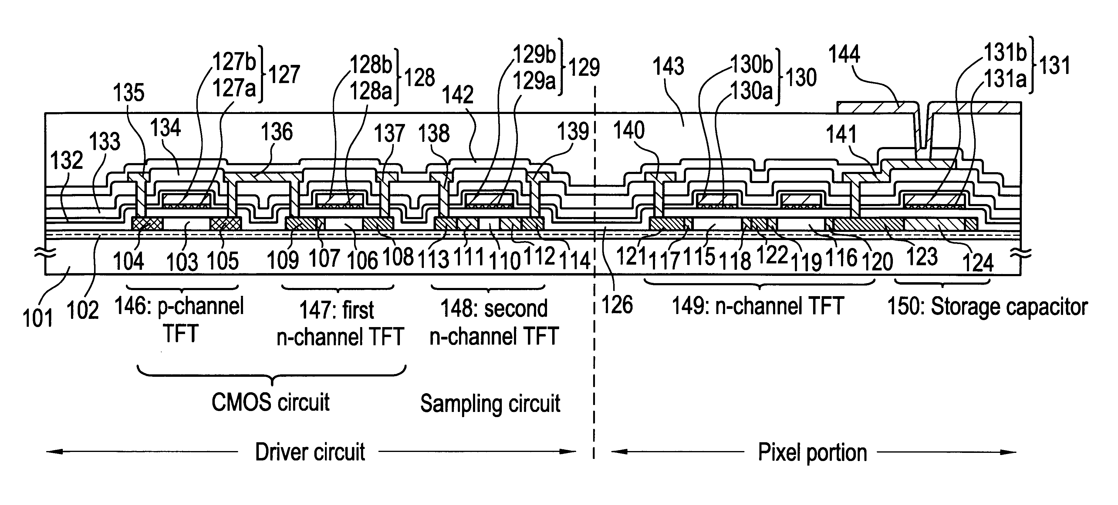
The present embodiment is described with reference to FIGS. 6A and 6B, and a method of simultaneously forming TFTs of the pixel portion and of the driver circuit provided on the periphery of the pixel portion differently from that in Embodiment 1 is described.

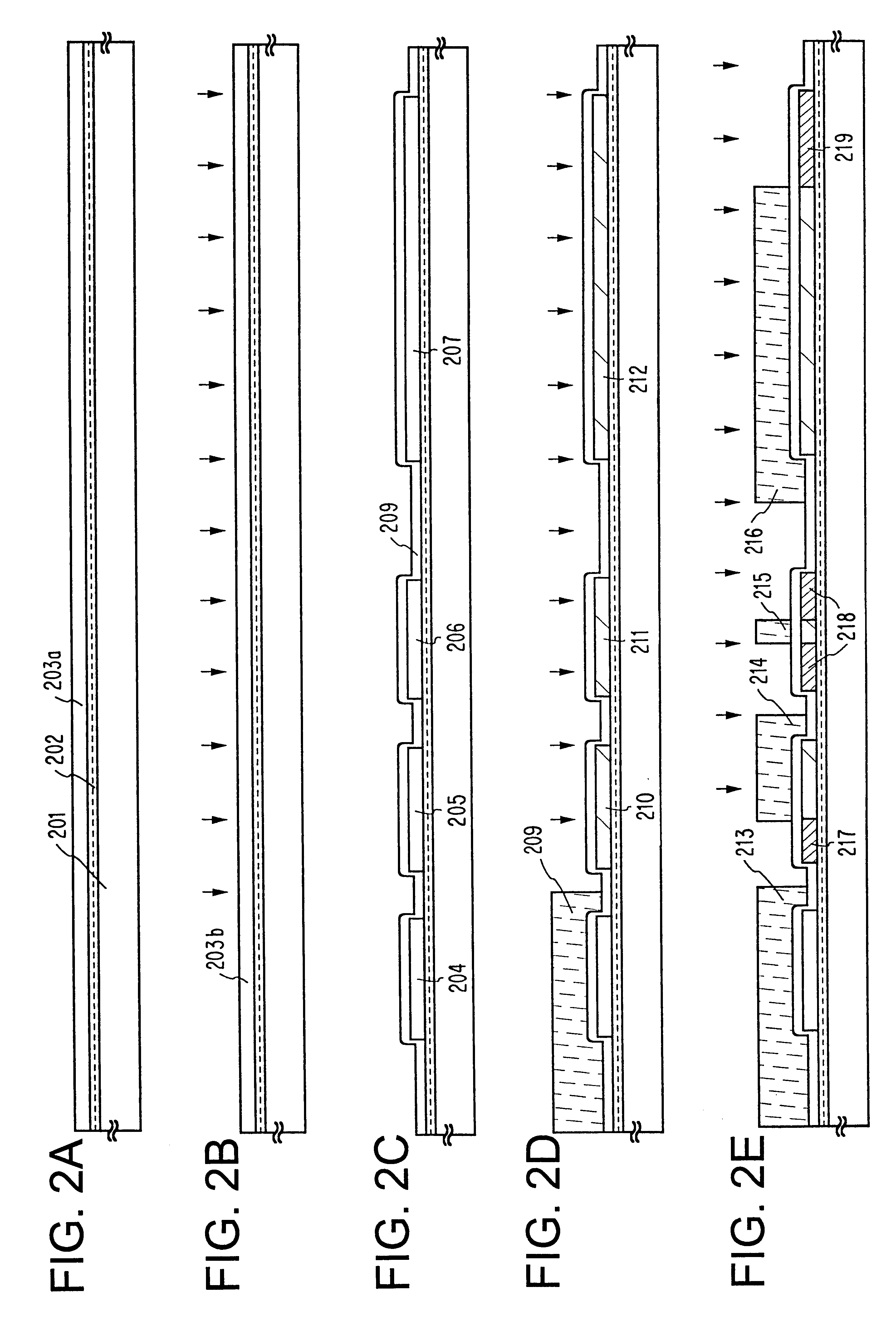
First, similarly to the case of Embodiment 1, the steps shown in FIGS. 2A to 3C are carried out. Then, a capping layer 301 is formed so as to cover at least the side surfaces of the gate electrodes 228 to 231. The capping layer is of a silicon nitride film, a silicon oxynitride film, or the like, and is formed at the thickness of from 25 to 200 nm. In the present embodiment, a silicon oxynitride film is formed by plasma CVD at the thickness of 100 nm. Then, an impurity element imparting n-type is doped by ion doping through the capping layer 301 into the island-like semiconductor layers thereunder to form impurity regions 303 to be LDD regions of the n-channel type TFT of the pixel portion. Here, the concentration of the doped ...

embodiment 3

The present embodiment is described with reference to FIGS. 13A to 13C, and another method of simultaneously forming TFTs of the pixel portion and of the driver circuit provided on the periphery of the pixel portion is described.

First, similarly to the case of Embodiment 1, the steps shown in FIGS. 2A to 4B are carried out. Here, in FIG. 13A, first wirings 403 and 404 are simultaneously formed from the same material as that of the gate electrodes. Insulating films 401 and 402 are formed from the same material as that of the gate insulating film 220. Then, the capping layer 248 is formed so as to cover at least the side surfaces of the gate electrodes. The capping layer is of silicon nitride film, silicon oxynitride film, or the like, and is formed at the thickness of 25 to 200 nm. In the present embodiment, a silicon oxynitride film is formed by plasma CVD at the thickness of 100 nm. Then, an impurity element imparting n-type is doped by ion doping through the capping layer 248 into...

embodiment 4

In the present embodiment, processes of manufacturing an active matrix liquid crystal display device from an active matrix substrate is described. As shown in FIG. 7, an alignment film 601 is formed onto the state of active matrix substrate of FIG. 5B fabricated in Embodiment 1. A polyimide resin is generally used for an alignment film of liquid crystal display devices. A shielding film 603, a transparent conductive film 604 and an alignment film 605 are formed on the opposing substrate 602 on the opposite side. After forming the alignment film, rubbing treatment is performed so that liquid crystal molecules are aligned at a determined pre-tilt angle. The active matrix substrate on which pixel section and CMOS circuits are formed, and the opposing substrate are such together through a sealing material and spacers etc. (neither is shown) by a known cell assembly process. Thereafter liquid crystal material 606 is injected between both substrates and completely sealed by a sealant (not...


PUM

PropertyMeasurementUnit
lengthaaaaaaaaaa
thicknessaaaaaaaaaa
thicknessaaaaaaaaaa

Abstract

By appropriately selecting the structure of top gate type or staggered type TFTs disposed in the respective circuits of a semiconductor device depending on the function of the circuits, the operating characteristics and the reliability of the semiconductor device is improved. An LDD region (107) the whole of which overlaps a gate electrode is provided in a first n-channel type TFT of a controlling circuit. LDD regions (111) and (112) at least part of which overlaps a gate electrode are provided in a second n-channel type TFT of the control circuit. LDD regions (117) to (120) which do not overlap a gate electrode through offset regions are provided in an n-channel type TFT of a pixel matrix circuit. By making different the concentration of LDD regions of the control circuit and the concentration of the pixel matrix circuit, optimized circuit operation is obtained.

Description

1. Field of the InventionThe present invention relates to a semiconductor device having a circuit formed of thin film transistors (hereinafter referred to as TFTs) over a substrate having an insulating surface, and to a method of manufacturing such a semiconductor device. In particular, the present invention is preferably utilized in an electro-optical device represented by a liquid crystal display device in which a pixel portion (or a pixel matrix circuit) and a driver circuit provided over the periphery of the pixel portion are provided over the same substrate, and in an electronic apparatus having such an electro-optical device mounted thereon. It is to be noted that a semiconductor device as used herein refers to any apparatus which functions by utilizing semiconductor characteristics, and includes the above-mentioned electro-optical device and electronic apparatus having such an electro-optical device mounted thereon.2. Description of the Related ArtSemiconductor devices having...

Claims


Application Information

Patent Timeline
Patent Type & Authority Patents(United States)
IPC IPC(8): H01L21/02H01L29/786H01L21/70H01L21/84H01L21/336H01L29/66H01L27/12G02F1/13G02F1/1362H01L27/28H01L21/316H01L27/32H01L21/77
CPCH01L27/1214H01L29/66757H01L29/78621H01L29/78627G02F1/13454H01L21/316H01L2029/7863H01L27/3244H01L27/127H10K59/12H01L21/02107
Inventor YAMAZAKI, SHUNPEI
Owner SEMICON ENERGY LAB CO LTD
Why Eureka
Try Eureka