

Method and system for pulse shaping in test and program modes
a pulse shaping and program mode technology, applied in the field of integrated circuits, can solve the problems of high pin count and increase the cost of an ic with the addition of charge-pumpes
- Summary
- Abstract
- Description
- Claims
- Application Information
AI Technical Summary
Problems solved by technology
Method used
Image

Examples
Embodiment Construction
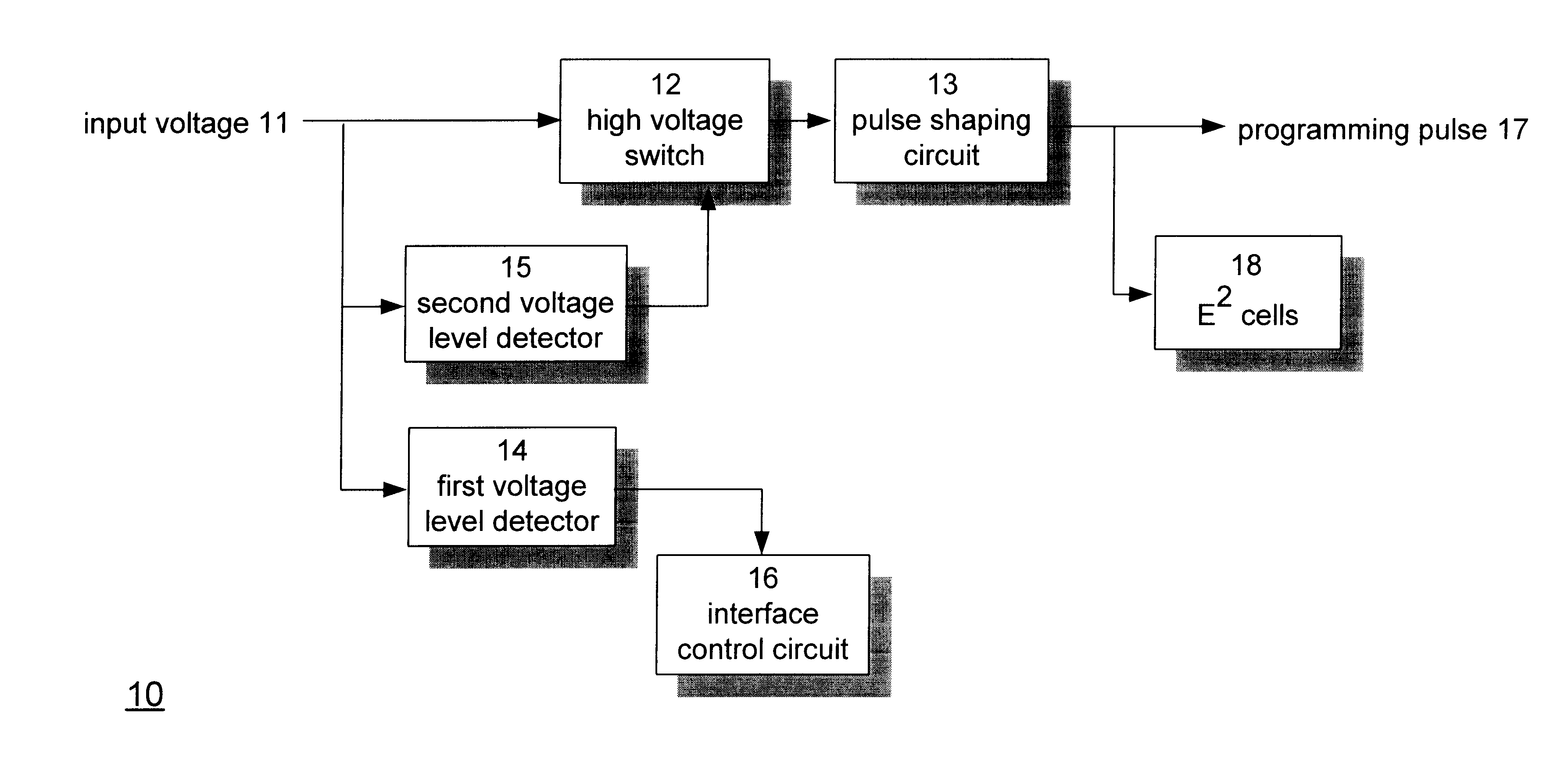
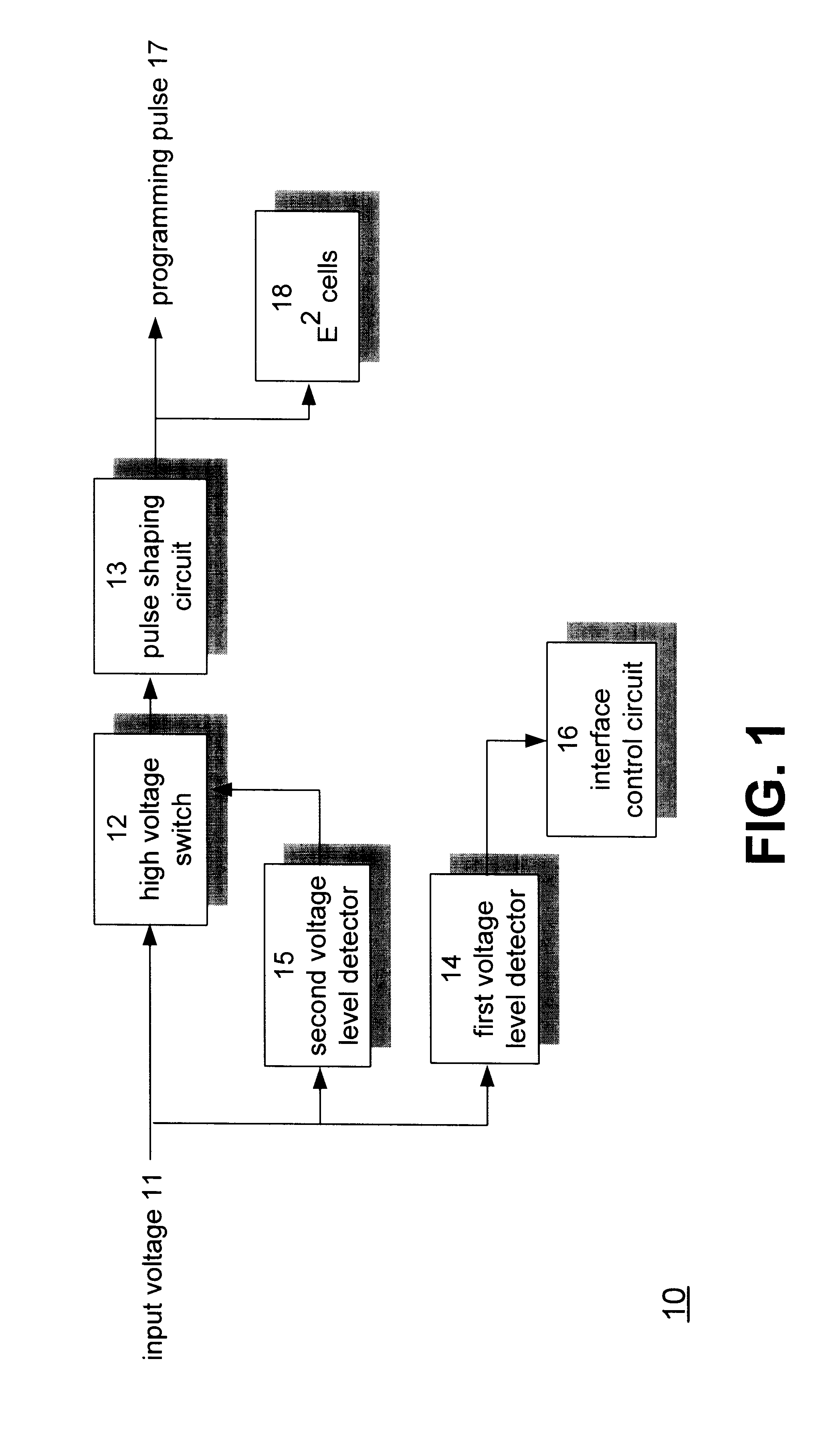
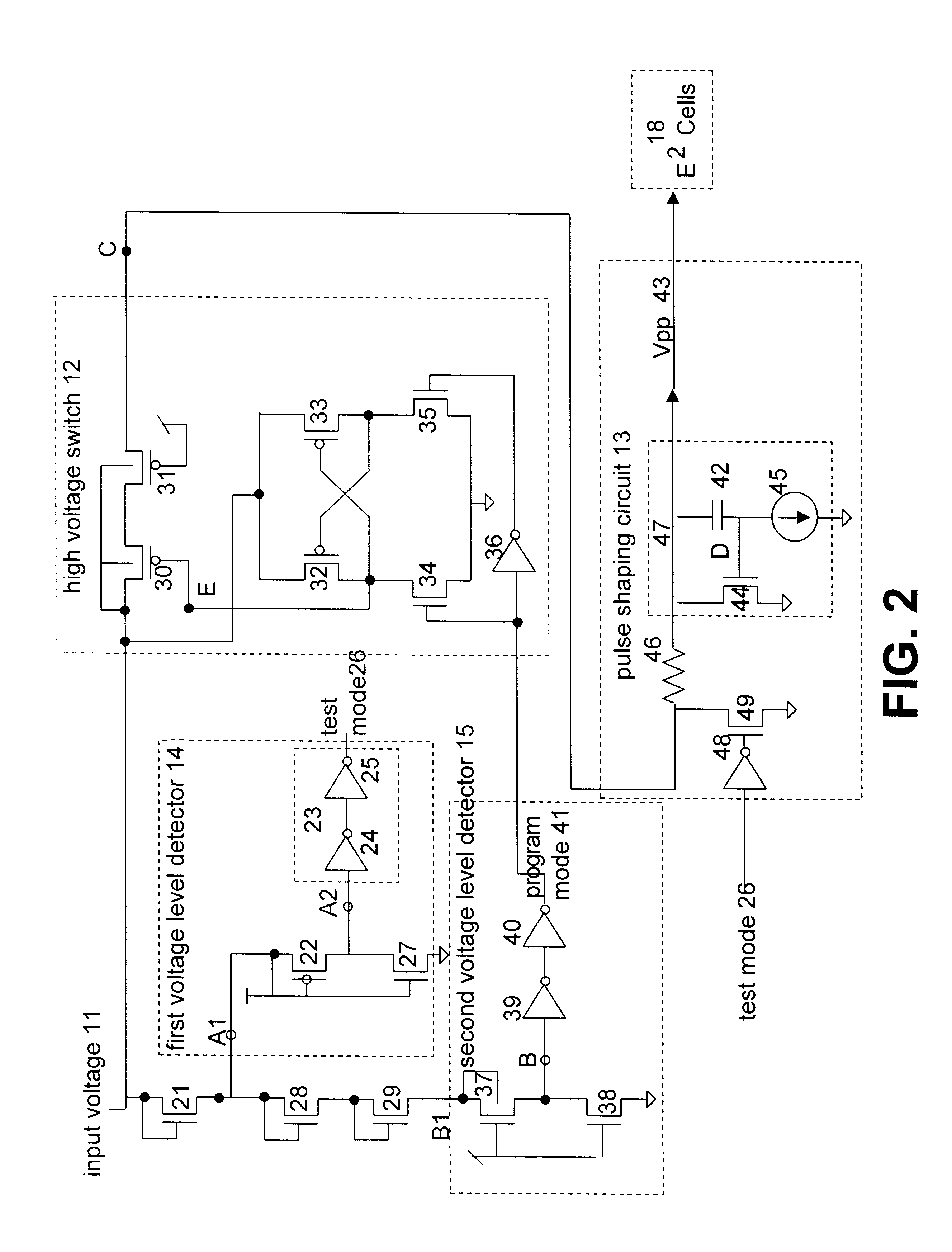
FIG. 1 is a block diagram illustrating an integrated circuit 10. An input voltage 11 is commonly fed to a high level switch 12, a first voltage level detector 14, and a second voltage level detector 15. Input voltage 11 is also referred to as test input pin or test input voltage. A pulse shaping circuit 13 couples to high-level switch 12 to provide a smooth transition when the voltage of test input pin increases to the second predetermined high voltage level to generate a programming pulse 17. While in test mode and not yet in a programming mode, an interface control circuit 16 allows test data or address information to enter into integrated circuit 10 for functional verification.
During a normal-mode operation, the input voltage 11 fluctuates between 0 to 5 volts, representing the nominal Vcc operating range. At that voltage range, the input voltage 11 is not at a sufficient high voltage level for the detection by either first voltage level detector 14 or second voltage level detect...
PUM
 Abstract
Description
Claims
Application Information