Pulse Shaping Circuit

a technology of electrical circuits and pulses, applied in pulse manipulation, pulse technique, instruments, etc., can solve the problems of time delay between off-on transition, time delay between laser or led turn-on and turn-off, and time delay associated with etc., to achieve the effect of reducing the time delay between laser or led turn-on and turn-o

Active Publication Date: 2007-05-10
LUMENTUM OPERATIONS LLC
View PDF15 Cites 9 Cited by
  • Summary
  • Abstract
  • Description
  • Claims
  • Application Information

AI Technical Summary

Benefits of technology

[0016] In accordance with another aspect of this invention, the pulse shaping electrical circuit further comprises a second high-pass filter circuit, a second variable offset circuit, and a second variable gain differential amplifier circui...

Problems solved by technology

There is, however, a time delay associated with switching the optical transmitter on or off, e.g. a time delay between an on-off transition in the drive current of the transmitter and an associated on-off transition in the light output thereof.
Similarly, there is a time delay between an off-on transition in the drive current of the transmitter and an associated off-on transition in the light output thereof.
This time delay can be seen as a consequence of a relatively large capacitance of a typical laser diode or light-emitting diode, which requires a certain time to be charged or discharged by the diode drive current, and/or a relatively large minority carrier life time in the active region of the diode.
The time delays associated with the laser or LED turn-on and turn-off are detrimental for higher-spee...

Method used


Image

  • Pulse Shaping Circuit
  • Pulse Shaping Circuit
  • Pulse Shaping Circuit

Examples


Embodiment Construction

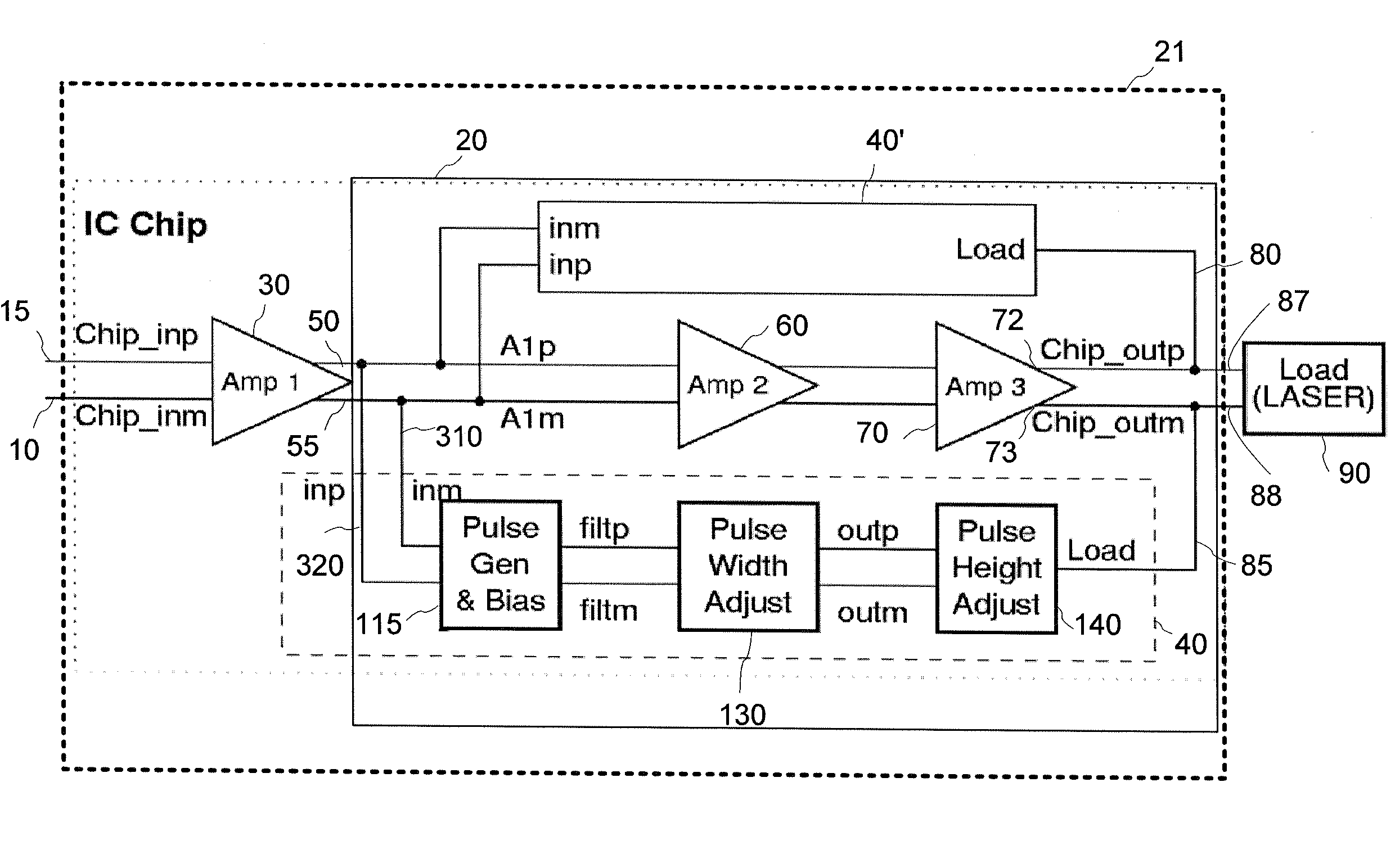
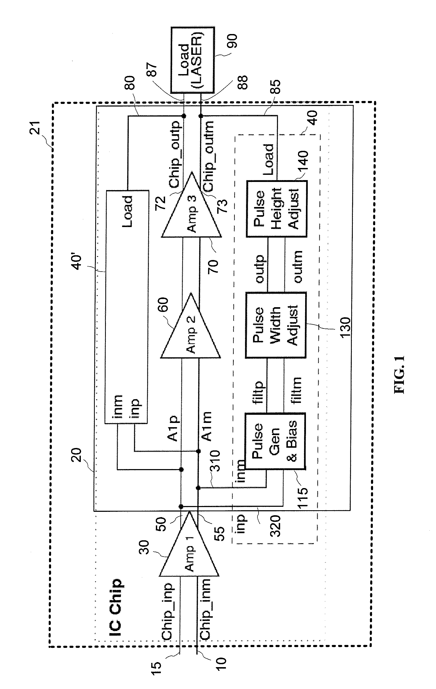
[0029] The present invention may be described herein in terms of various functional components. It should be appreciated that such functional components may be realized by any number of hardware or structural components configured to perform the specified functions. For example, the present invention may employ various integrated components comprised of various electrical devices, e.g., resistors, transistors, capacitors, diodes and the like, whose values may be suitably configured for various intended purposes. Further, it should be noted that while various components may be suitably coupled or connected to other components within exemplary circuits, such connections and couplings can be realized by direct connection between components, or by connection through other components and devices. Also, for ease of explanation and understanding of the present invention, superfluous details have not been included.

[0030] An exemplary embodiment of the pulse shaping circuit according to the...


PUM


Abstract

The invention relates to a pulse shaping circuit for shaping electrical pulses driving an optical transmitter, e.g. a lased diode or an LED, and for providing electrical pulses having independently height and width-adjustable peaking at the edges thereof. The pulse shaping circuit of the present invention includes a high-pass RC filter with a differential output for providing transient electrical pulses from an input differential pulse, an adjustable voltage offset generating circuit, a differential amplifier for adjusting the width of the transient electrical pulses in dependence on the adjustable voltage offset, and a variable-gain current-steering amplifier for producing transient pulses with independently adjustable width and height.

Description

CROSS-REFERENCE TO RELATED APPLICATIONS [0001] The present invention claims priority from U.S. Patent Application No. 60 / 734,073 filed Nov. 7, 2005, which is incorporated herein by reference for all purposes.TECHNICAL FIELD [0002] The present invention relates to a pulse shaping electrical circuit, and in particular to a circuit that adds width and height adjustable peaking to pulse edges. BACKGROUND OF THE INVENTION [0003] There are many applications in which an optical transmitter, such as a laser diode (LD) or a light-emitting diode (LED), is driven by a pulsed electrical current to alternately switch the light source on and off, and to produce optical pulses. [0004] Typically, it is desired that the optical pulses be of a substantially rectangular shape and follow the current pulses as closely as possible. There is, however, a time delay associated with switching the optical transmitter on or off, e.g. a time delay between an on-off transition in the drive current of the transmi...

Claims


Application Information

Patent Timeline
IPC IPC(8): H01S3/13
CPCH01S5/042H03K5/06H03K5/12
Inventor BAUMGARTNER, STEVEN J.NATZKE, BRAD ANTHONY
Owner LUMENTUM OPERATIONS LLC
Why Eureka
Try Eureka