

Modified current mirror circuit for BiCMOS application
a current mirror and circuit technology, applied in the direction of electric variable regulation, process and machine control, instruments, etc., can solve the problem of current mirror mosfet device to turn off during the operation
- Summary
- Abstract
- Description
- Claims
- Application Information
AI Technical Summary
Benefits of technology
Problems solved by technology
Method used
Image

Examples
first embodiment
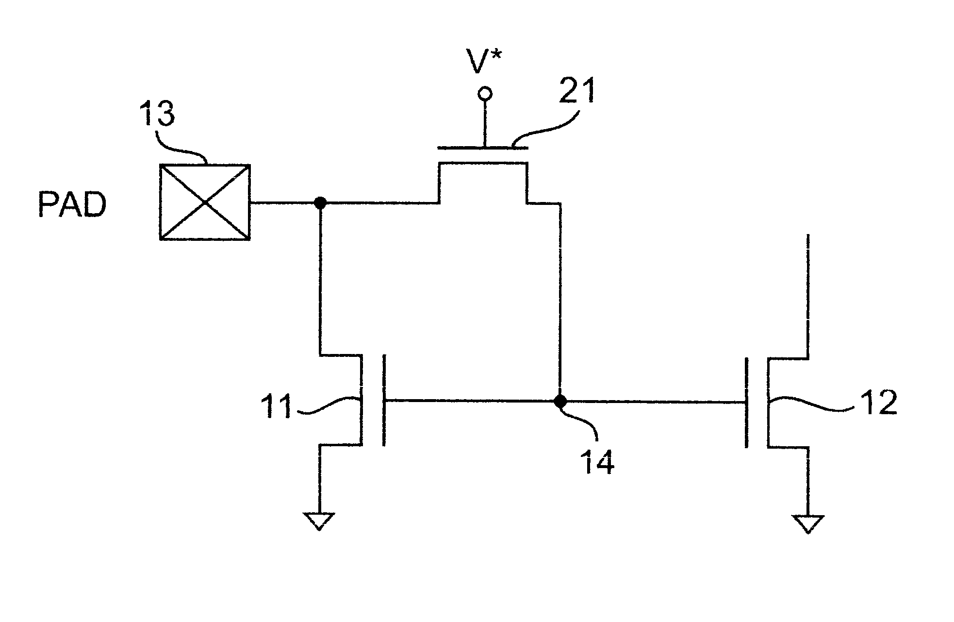
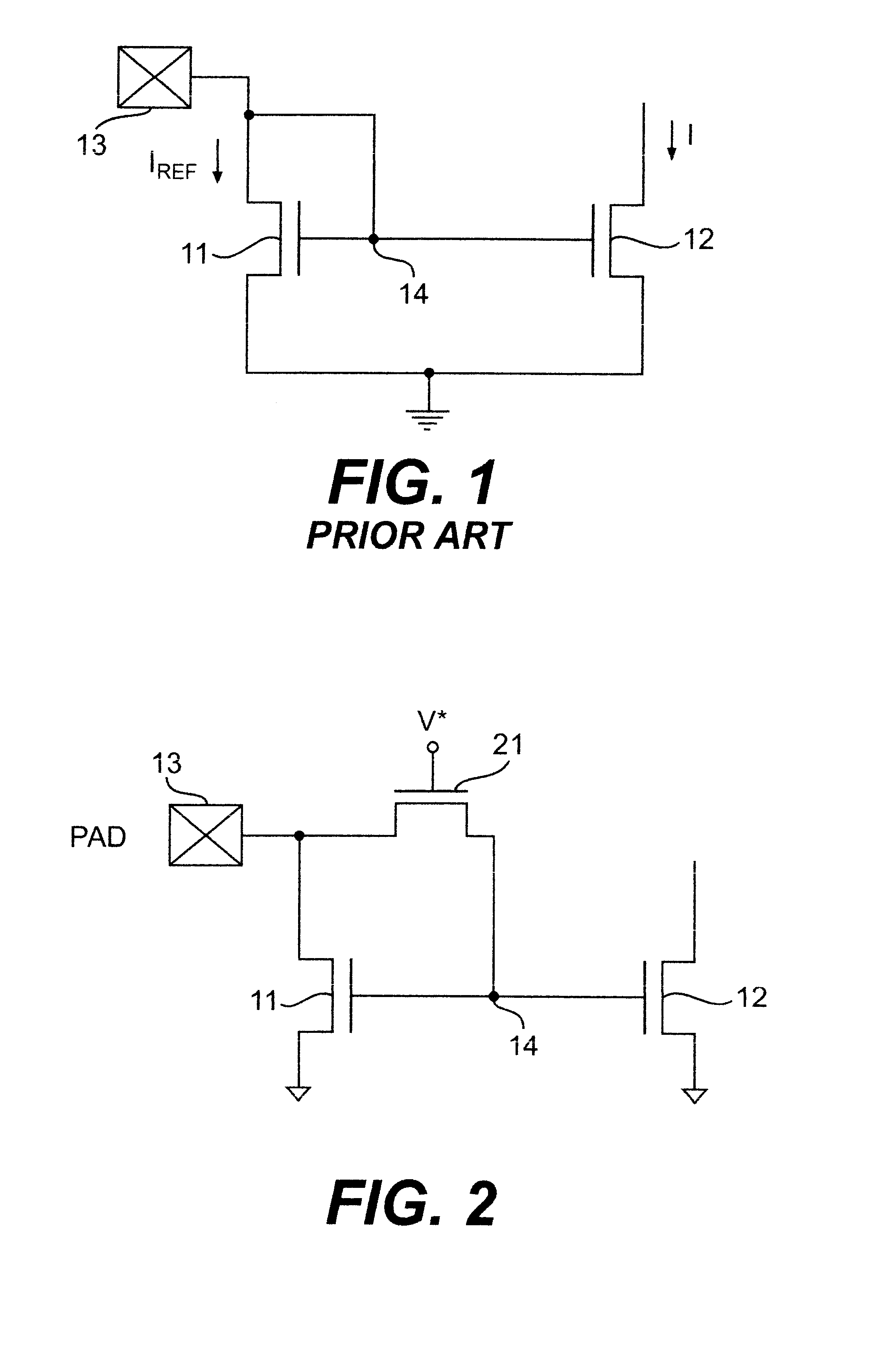
In the invention, the conventional current mirror circuit shown in FIG. 1 is modified as shown in FIG. 2 to provide a means of decoupling the common or gate node 14 when the chip is unpowered. In this case, an FET 21 is substituted for the direct connection between common node 14, to which the gates of the FETs 11 and 12 are connected and the source of the FET 11. The source of the FET 21 is connected in common with the source of FET 11 to the pad 13, while the drain of FET 21 is connected to common node 14. The gate of FET 21 is connected to a voltage V*.
The voltage V* is a reference voltage, a power rail voltage or connected to additional logic. When the chip is unpowered, V* is at a low potential. As voltage is applied to pad 13, the FET 21 remains off. The FET 11 will not be turned on until the voltage applied to pad 13 exceeds the avalanche breakdown voltage of FET 21.
second embodiment
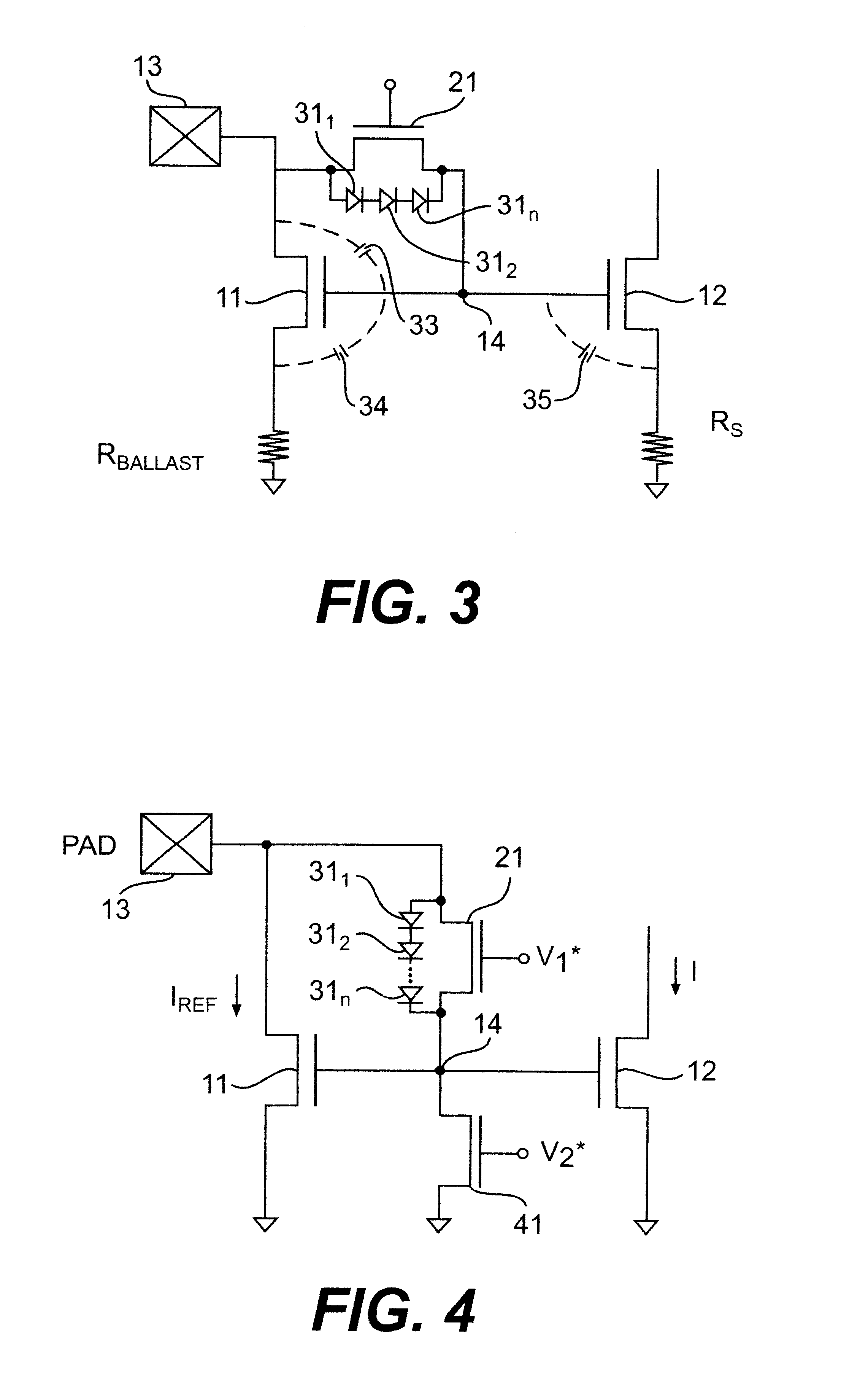
In the invention, the circuit of FIG. 2 is further modified in the circuit shown in FIG. 3 by the addition of a series of diodes 31.sub.1, 31.sub.2, . . . , 31.sub.n connected in parallel with the source-drain circuit of FET 21, a ballast resistor R.sub.Ballast in the drain circuit of FET 11, and a resistor R.sub.s in the drain circuit of FET 12. The diodes 31.sub.1 to 31.sub.n provide over voltage protection for FET 21 as well as a turn on state voltage V'. This diagram also shows the parasitic capacitances 33 between the source and gate of FET 11, 34 between the gate and drain of FET 11, and 35 between the gate and drain of FET 12. The turn-on voltage of the series of the diodes 31.sub.1, 31.sub.2, . . . , 31.sub.n is ##EQU1##
where n is the number of diodes, V.sub.f =0.7V and I.sup.2 is the parasitic bipolar gain of the PNP structure of the diode element. When V.sub.av of the FET 21 is greater than V.sub.diode, current will flow to the node 14, allowing the gate of the FET 11 to r...
third embodiment
A further modification of the circuit according to the invention is shown in FIG. 4. In this case, an additional FET 41 is added between the node 14 and circuit ground, with the source of FET 41 being connected to node 14 and the drain connected to circuit ground. The gate of FET 21 is connected to voltage V*.sub.1, and the gate of FET 41 is connected to voltage V*.sub.2. Voltage V*.sub.1 is operational in ESD mode to turn FET 21 off. Normally, FET 21 is on or conducting. Voltage V*.sub.2 is operational in ESD mode to turn FET 41 on to hold down the gate electrodes of FETs 11 and 12. Normally, FET 41 is off or non-conducting. There are N diodes 31.sub.1 to 31.sub.n to allow over driving of V*.sub.2 allowing the gates of FETs 11 and 12 to rise after a set voltage level.
A conventional bipolar circuit is shown in FIG. 5. This circuit comprises two NPN transistors 51 and 52. The collector of transistor 51 is connected to a pad 53, which is the source of a reference current I.sub.Ref, an...
PUM
 Abstract
Description
Claims
Application Information