Manufacturing method for integrated sensor arrays

a manufacturing method and sensor array technology, applied in the direction of instruments, electrical equipment, material analysis, etc., can solve the problems of contaminated top layers, contaminated top layers, and small amounts of resist in the to player electrode or its substrate, and seriously impair the sensor recognition ability

a manufacturing method and sensor array technology, applied in the direction of instruments, electrical equipment, material analysis, etc., can solve the problems of contaminated top layers, contaminated top layers, and small amounts of resist in the to player electrode or its substrate, and seriously impair the sensor recognition ability

US6410445B1Inactive Publication Date: 2002-06-25APPLIEDSENSOR SWEDEN

Image

  • Manufacturing method for integrated sensor arrays
  • Manufacturing method for integrated sensor arrays
  • Manufacturing method for integrated sensor arrays

Examples


Embodiment Construction

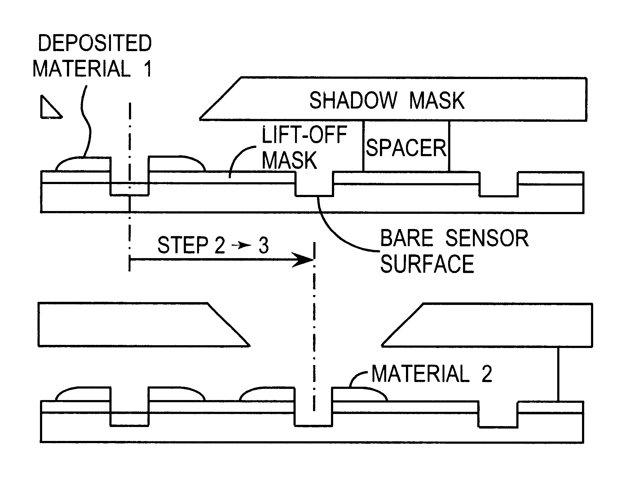
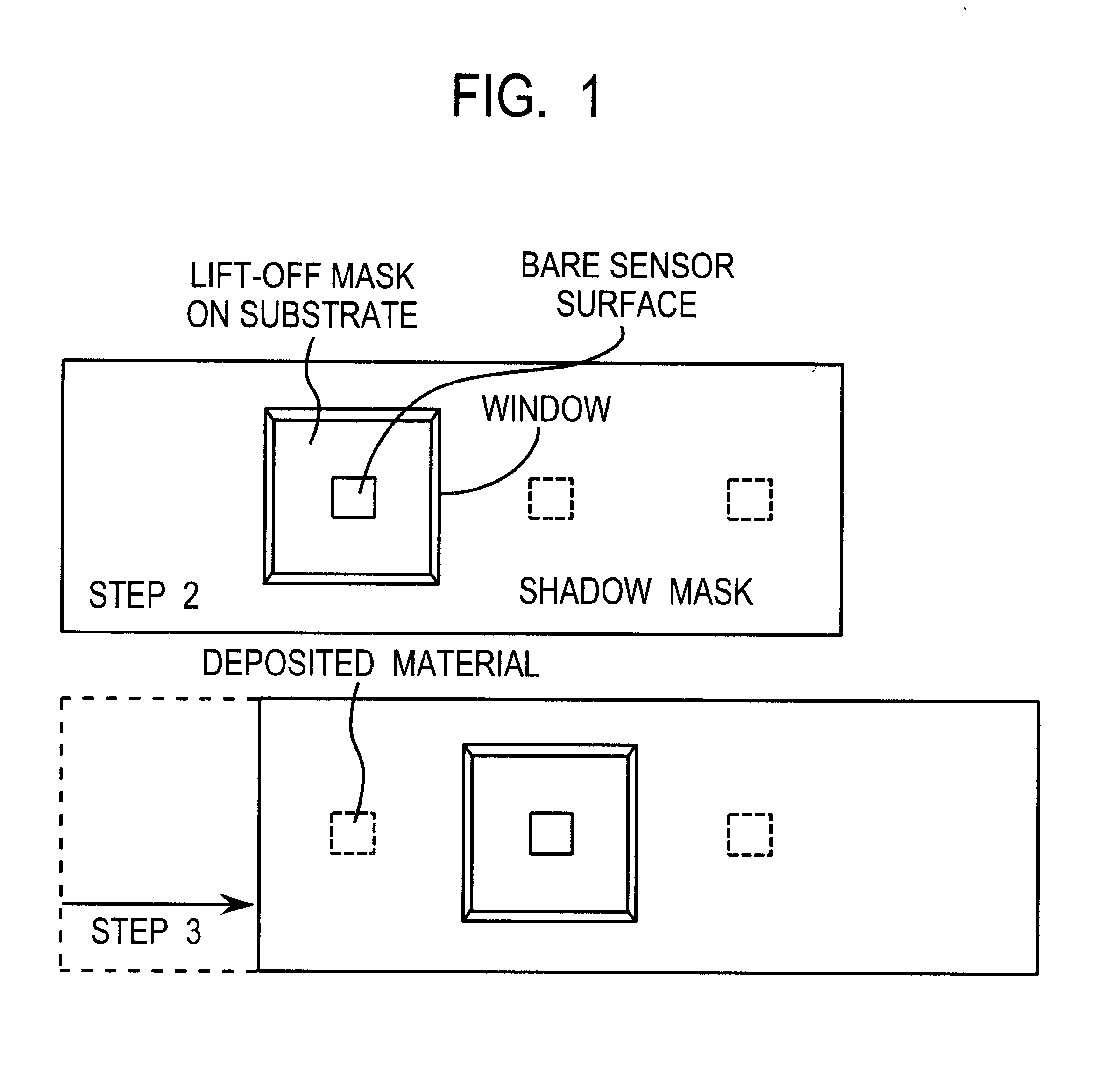
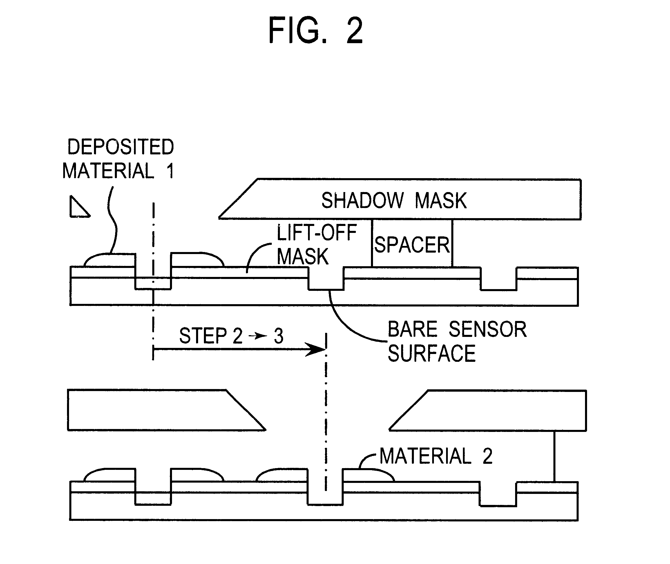
Step 1. The entire substrate wafer is subjected to the first part of a single lift-off procedure resulting in a resist layer with openings for all the top-layer sensor surfaces where the sensing layer material is to be deposited.

Step 2. The wafer is additionally covered by a shadow mask with only one mask window for each sensor of a first type in the array. The windows are larger than the resist openings and the windows are situated so that the mask can be placed with one window over each opening in the resist where deposition of a layer of a first type is intended (note that there can be more than one sensor of the same type in each array). The first material is deposited, e.g., by evaporation or sputtering in a vacuum chamber.

Step 3. The shadow mask is then moved so that its windows are located where a second type of sensor may be located in the array (see FIGS. 1 and 2). Then the next or second electrode material is deposited in and close to the openings in the resist.

Step 3 is r...


PUM

PropertyMeasurementUnit
areasaaaaaaaaaa
areaaaaaaaaaaa
distanceaaaaaaaaaa

Abstract

Method for the fabrication of sensor arrays with individually different sensing surface, where lift off technique and shadow mask technique is used simultaneously. A resist layer with openings at all locations where coatings are intended is applied with lift off technique. Then a shadow mask is used provided with widows only at the openings where deposit is intended for one specific coating. By for instance vapor deposition, coatings are effected where there are openings in the resist and windows in the shadow mask. The shadow mask is moved to the next depositions location and the procedure repeated until all coatings have been effected. The shadow mask is removed as is also the resist giving an improved sensor quality compared to prior-art methods.

Description

The present invention relates to a method for manufacturing integrated arrays of sensors, in particular chemical sensors or physical sensors e.g., field-effect chemical sensors. Such sensors are typically based on metal-insulator-semiconductor or metal-conductor structures. The present invention improves the quality of the top layer that serves as the chemically sensitive part of the device.1. IntroductionIt is known that catalytic metals can be used as gate electrodes for chemically sensitive field-effect devices such as transistors, capacitors, diodes, etc. These metal-insulator-semiconductor or metal-semiconductor devices may be used to measure small concentrations of molecules in the gas phase or ions in the liquid phase. The parameters that are normally changed when manufacturing field-effect sensors with different sensitivities towards different chemical compounds are the material and thickness of the top electrode. In this way the individual sensors in an array can be made se...

Claims


Application Information

Patent Timeline
25 Jun 2002
Publication
US6410445B1
IPC
G01N27/403; G01N27/414; G03F7/00
CPC
G01N27/414; G03F7/0007
Inventors
FAGERMAN, PER-ERIK