Semiconductor memory device and reading and writing method thereof

Inactive Publication Date: 2002-07-16
RENESAS ELECTRONICS CORP
View PDF5 Cites 68 Cited by
  • Summary
  • Abstract
  • Description
  • Claims
  • Application Information

AI Technical Summary

Problems solved by technology

Thus, increases in costs of the entire device including controllers and other members are unavoidable.
In case read commands or write commands are executed in each buffer size while these buffer sizes remained smal

Method used


Image

  • Semiconductor memory device and reading and writing method thereof
  • Semiconductor memory device and reading and writing method thereof
  • Semiconductor memory device and reading and writing method thereof

Examples


Example

The first embodiment of 
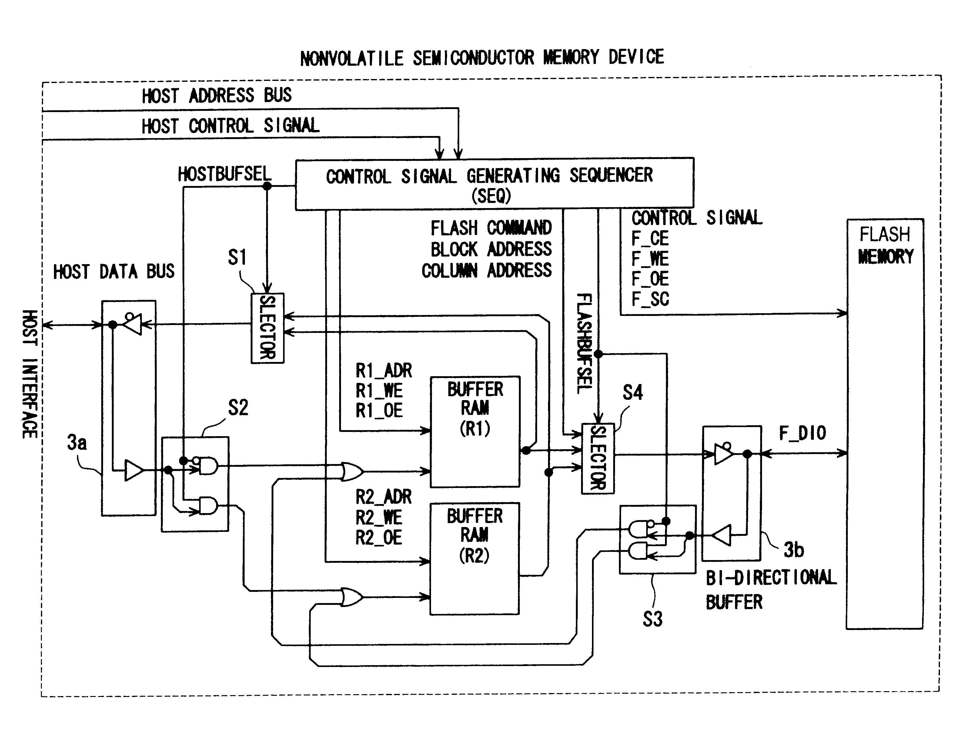
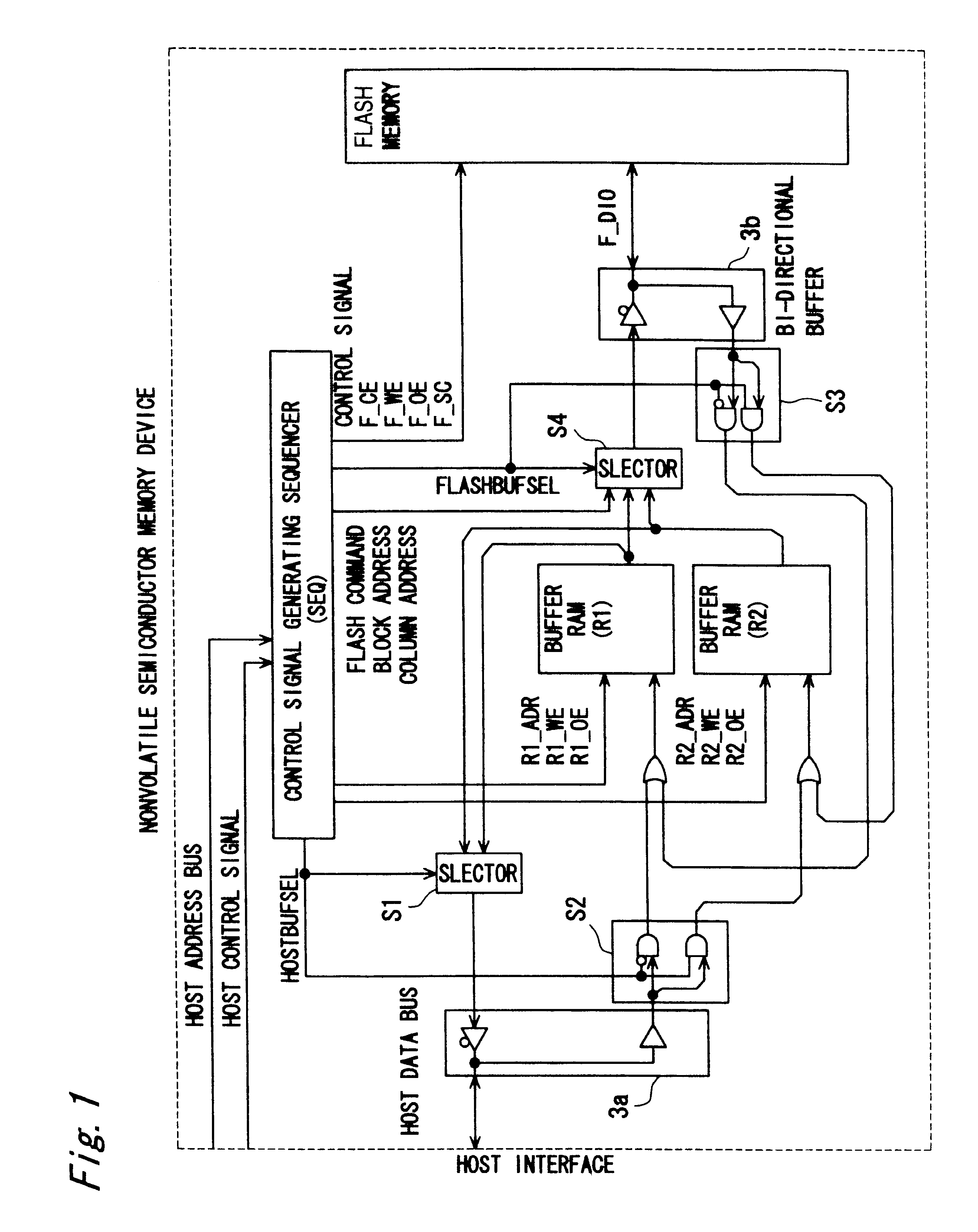
the present invention will now be explained with reference to FIGS. 1 to 5. It should be noted that elements that are common to these drawings are marked with identical reference numerals, and that repetitive explanations are omitted.

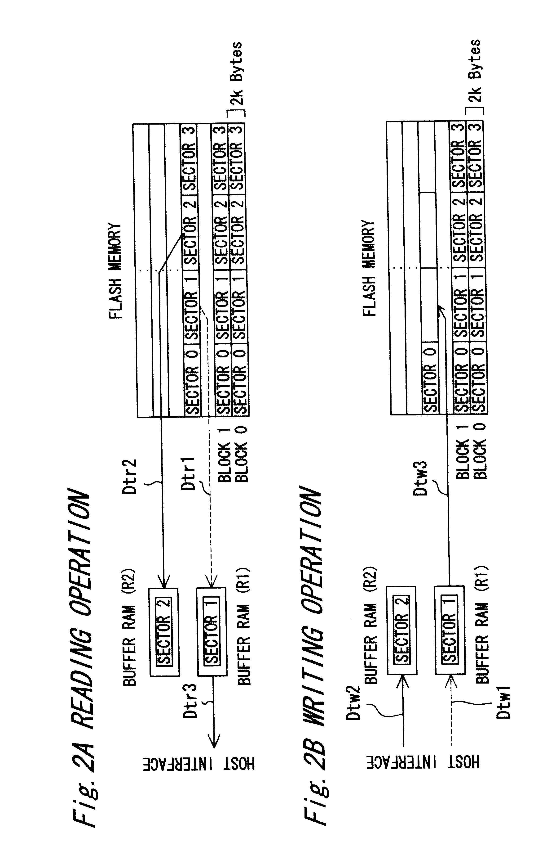
FIG. 1 illustrates a block structure of a semiconductor memory device according to a first embodiment using a nonvolatile semiconductor memory of the present invention. In this drawing, the semiconductor memory device is comprised of a control signal generating sequencer (SEQ) 1 serving as a control signal generating means, a flash memory 2 arranged to be of a hierarchical structure including a plurality of blocks, two buffer RAMs (R1, R2), two bidirectional buffers 3a and 3b, and four selectors S1, S2, S3, S4. Each buffer RAM (R1, R2) is connected to a host interface portion 4 by a host data bus via the selectors S1 and S2 and via the bidirectional buffer 3a so as to enable reading and writing of data from and to the host termin...

Example

The second embodiment of the present invention will now be explained with reference to FIG. 6. The structural differences between the second embodiment and the first embodiment reside in the provision of an error correction controlling unit (ECC) 5 in the second embodiment. As illustrated in FIG. 6, the error correction controlling unit (ECC) 5 is interposed between the selectors S3, S4 and the bidirectional buffer 3b and is connected across the data bus lines DI and DO. Thus, redundant data for error correction may be transmitted to the error correction controlling unit (ECC) 5 together with sector data in parallel with read out data from the flash memory 2 to the buffer RAMs (R1, R2). Thus, when correctable errors shall be detected, data may be corrected-on the buffer RAM.

When performing a write operation of data from the buffer RAM to the flash memory, sector data is transmitted to the error correction controlling unit (ECC) 5 in parallel therewith to generate redundant data, and...


PUM


Abstract

A capacity size of a single block of a flash memory (2) is an integer multiple of a single sector size which is a processing unit of an external host (4), and each of the first and second buffer RAMs interposed between the external host and the flash memory has a capacity corresponding to a single sector size of the flash memory, and data transmission between the external host and the buffer RAMs and between the flash memory and the buffer RAMs are performed by alternately selecting different buffer RAMs, and thus the data transmission between the buffer RAMs and the external host is performed simultaneously. and in parallel with performing the data transmission between the buffer RAMs and the flash memory.

Description

1. Field of the InventionThe present invention relates to a semiconductor memory device, and particularly to a semiconductor memory device of large capacity such as a semiconductor disk device employing a flash memory in which reading, writing and erasing are performed in block units, and employing a memory of a large capacity as a nonvolatile semiconductor memory for realizing high performance with reduction in manufacturing costs.2. Description of the Prior ArtExamples of conventionally used nonvolatile semiconductor memories are, for instance, M5M29F25611VP manufactured by Mitsubishi Electric Corporation and HN29W25611 manufactured by Hitachi Ltd., which are flash memories performing read and write processes in block units of 2 k bytes. In a semiconductor memory device mounted with such a flash memory, the flash memory includes a plurality of blocks each of which are of 2 k bytes as illustrated in FIG. 7 for enabling parallel processing of data transmission to / from the host termi...

Claims


Application Information

Patent Timeline
IPC IPC(8): G11C8/12G11C8/00G11C7/10G11C16/06G06F12/16G06F12/00G11C16/02
CPCG11C7/1051G11C7/1078G11C7/1087G11C8/12G11C16/06
Inventor YOSHIMURA, YOSHIMASA
Owner RENESAS ELECTRONICS CORP
Why Eureka
Try Eureka