Printed circuit board with heat spreader and method of making

a technology of printed circuit boards and heat spreaders, which is applied in the direction of printed circuit assembling, printed circuit manufacturing, electric connection formation of printed elements, etc., can solve the problem of reducing the internal thermal resistance (.theta..sub.jc) of the packag

Inactive Publication Date: 2002-09-10
AMKOR TECH SINGAPORE HLDG PTE LTD
View PDF8 Cites 34 Cited by
  • Summary
  • Abstract
  • Description
  • Claims
  • Application Information

AI Technical Summary

Problems solved by technology

The authors claim that this design reduces the internal thermal resistance (.THETA..sub.jc) of the package to a value that is typically less than 1 degree C / Watt for most sizes of chip.

Method used


Image

  • Printed circuit board with heat spreader and method of making
  • Printed circuit board with heat spreader and method of making
  • Printed circuit board with heat spreader and method of making

Examples


Embodiment Construction

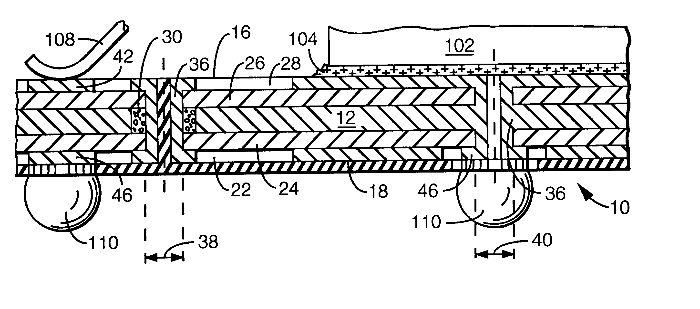
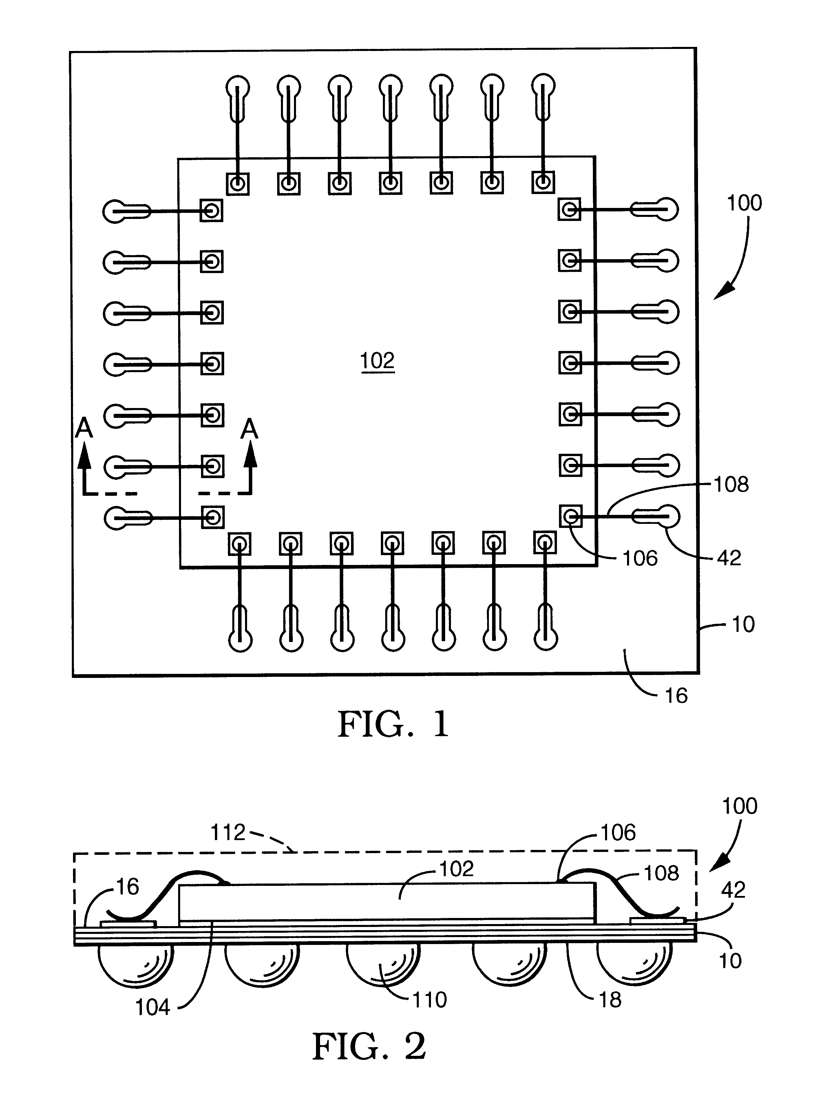
An exemplary embodiment of a PCB 10 with a heat spreader 12 in accordance with the present invention is illustrated in the context of a PBGA-type of semiconductor package 100 in FIGS. 1-3. In the exemplary embodiment, a semiconductor die, or "chip" 102, is shown attached to the upper surface 16 of the PCB 10 with, e.g., a layer 104 of solder or a filled epoxy (see also FIG. 7).

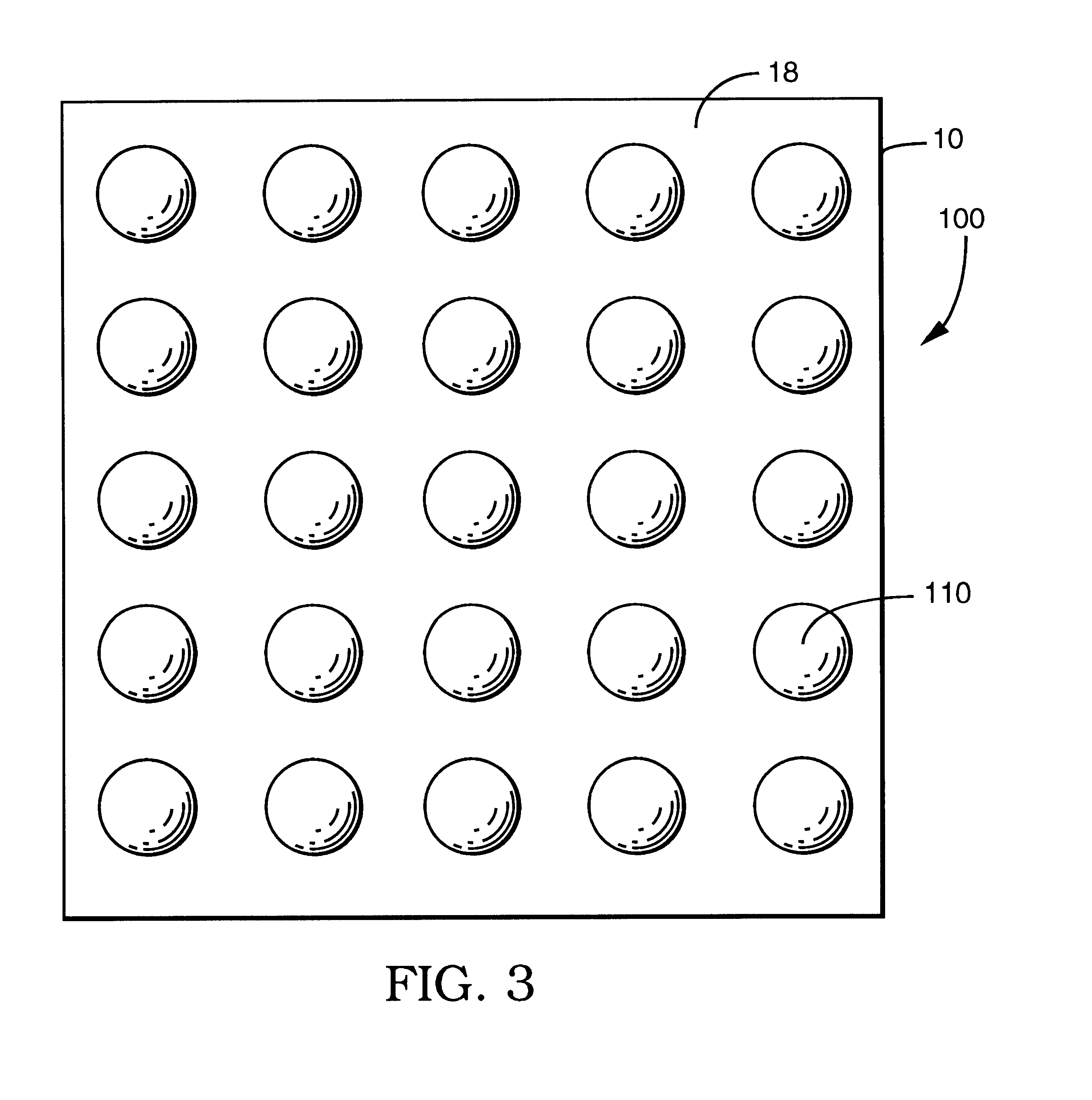
Die pads 106 on the chip 102 are electrically connected to corresponding pads 42 on the PCB 10 by fine, conductive wires 108 having opposite ends respectively bonded to corresponding ones of the pads on the die and the PCB. Electrical signals are conducted from the die pads 106 through the wires 108 to the pads 42 on the PCB, and thence, through the PCB by "vias," i.e., plated-through apertures in the PCB, to lands 46 (FIG. 7) on the lower surface 18 of the PCB. Solder balls 110 are welded on the lands 46 to serve as input / output terminals or heat conducting terminals of the package 100. A monolithic body 112 ...


PUM

PropertyMeasurementUnit
thickaaaaaaaaaa
diameteraaaaaaaaaa
diameteraaaaaaaaaa

Abstract

A method of making a PCB having an integral heat spreader and/or central ground plane includes forming one or more first openings in a first layer of a metal at selected locations and filling the. openings with an electrically insulating material. The first sheet is laminated between second and third layers of a metal interleaved with first and second layers of a dielectric material. At least one second opening is formed through the insulating material in one of the first openings, and at least one third opening is formed in the laminate at a position displaced from the first openings. The upper and lower layers of metal are electrically connected to each other through the at least one second and third openings to define "vias" through the laminate. The vias comprise "clearance vias" from which the first metal sheet is electrically isolated, and "thermal vias" to which the first metal sheet is electrically connected. The thermally enhanced PCB is fabricated using only conventional PCB fabrication techniques.

Description

1. Field of the InventionThis invention relates to printed circuit boards ("PCBs") in general, and in particular, to a PCB with an integral heat spreader for use in semiconductor packages and a method of making such a PCB.2. Description of the Related ArtTo be practically useful, semiconductor chips are typically housed in robust packages that protect them from the environment, permit them to be reliably interconnected with associated components, and enable them to effectively dissipate heat to the ambient.The current trend toward electronic devices that are more compact, yet faster and more functional, has created a corresponding demand for semiconductor packages that are smaller, yet which permit a more dense mounting of components dissipating greater amounts of heat. One response to this demand has been the development of so-called ball grid array ("BGA"), land grid array ("LGA"), and lead-less chip carrier ("LCC") types of packages that substitute lands or balls of solder on the...

Claims


Application Information

Patent Timeline
Patent Type & Authority Patents(United States)
IPC IPC(8): H01L21/02H01L21/48H05K3/44H05K3/42H01R12/04
CPCH01L21/4857H05K3/445H01L2224/48091H01L2224/48227H01L2224/48465H01L2224/49175H01L2924/01078Y10T29/49126H01L2924/15311H05K3/427H01L2924/01079H01L2924/00014H01L2924/00H01L2224/05554H01L2224/73265H01L2924/181H01L2924/00012
Inventor HUEMOELLER, RONALD P.
Owner AMKOR TECH SINGAPORE HLDG PTE LTD
Why Eureka
Try Eureka