Apparatus and method for evaluating semiconductor structures and devices

a semiconductor and structure technology, applied in the field of electromechanical devices, can solve the problems of inability to manufacture integrated circuits, inability to inhibit the production of semiconductor devices, and infancy of semiconductor fabrication processes, and achieve the effect of reducing disadvantages and problems associated with semiconductor devices

Inactive Publication Date: 2002-12-24
TEXAS INSTR INC
View PDF5 Cites 14 Cited by
  • Summary
  • Abstract
  • Description
  • Claims
  • Application Information

AI Technical Summary

Benefits of technology

In accordance with the present invention, an apparatus and methods are provided which substantially eliminates or reduces disadvantages and problems associated with prior device evaluation methods and apparatuses.

Problems solved by technology

Semiconductor fabrication processes, in their infancy, were sometimes plagued with fatal defectivity that inhibited the production of integrated circuits.
As semiconductor fabrication processes became more advanced, the level and occurrence of defects in semiconductor devices have decreased.
However, the reduction of semiconductor geometries to submicron levels has manifested inherent defect modes which may impact the performance of resulting semiconductor devices.
Structural defects are one of the inherent problems facing the advancement of submicron semiconductor devices.
Some structural defects negatively impact device performance and may effect, for example, leakage currents, carrier lifetimes, and gate oxide integrity.
One defect that occurs in semiconductor processing is an area defect called grain boundaries.
As a result, any two layers may have an angle of misorientation that occurs during a single process.
This causes a dislocation between the two layers resulting in a grain boundary.
Another defect that occurs in semiconductors is caused by voids in the lattice material due to precipitates of extrinsic or intrinsic point defects.
A bulk defect that occurs in one silicon crystal layer can be the cause of other crystalline defects as additional layers are grown.
Consequently, the lattice surrounding the silicon dioxide precipitate is subject to large compressions placing undue stress on the lattice and junction regions which can lead to a bulk defect within the lattice structure.

Method used


Image

  • Apparatus and method for evaluating semiconductor structures and devices
  • Apparatus and method for evaluating semiconductor structures and devices
  • Apparatus and method for evaluating semiconductor structures and devices

Examples


Embodiment Construction

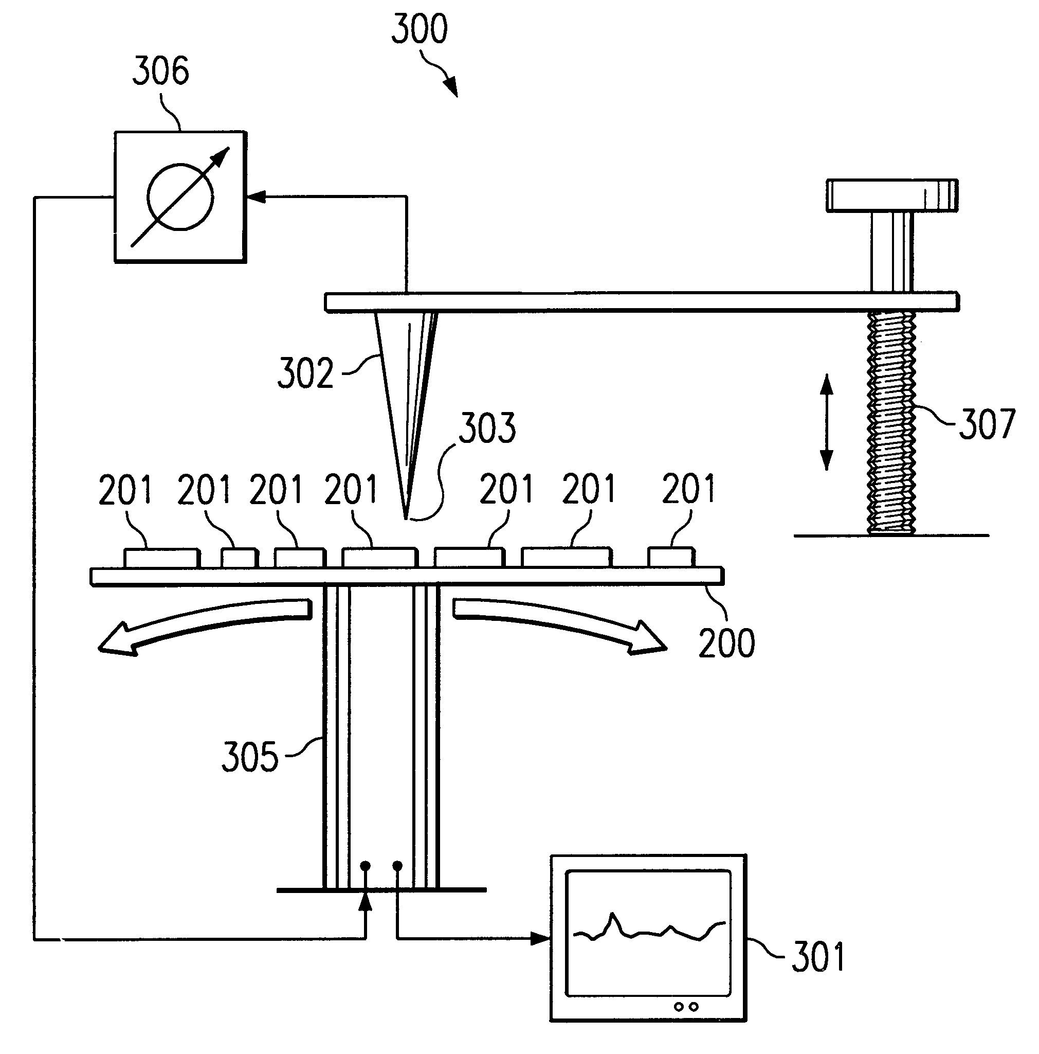
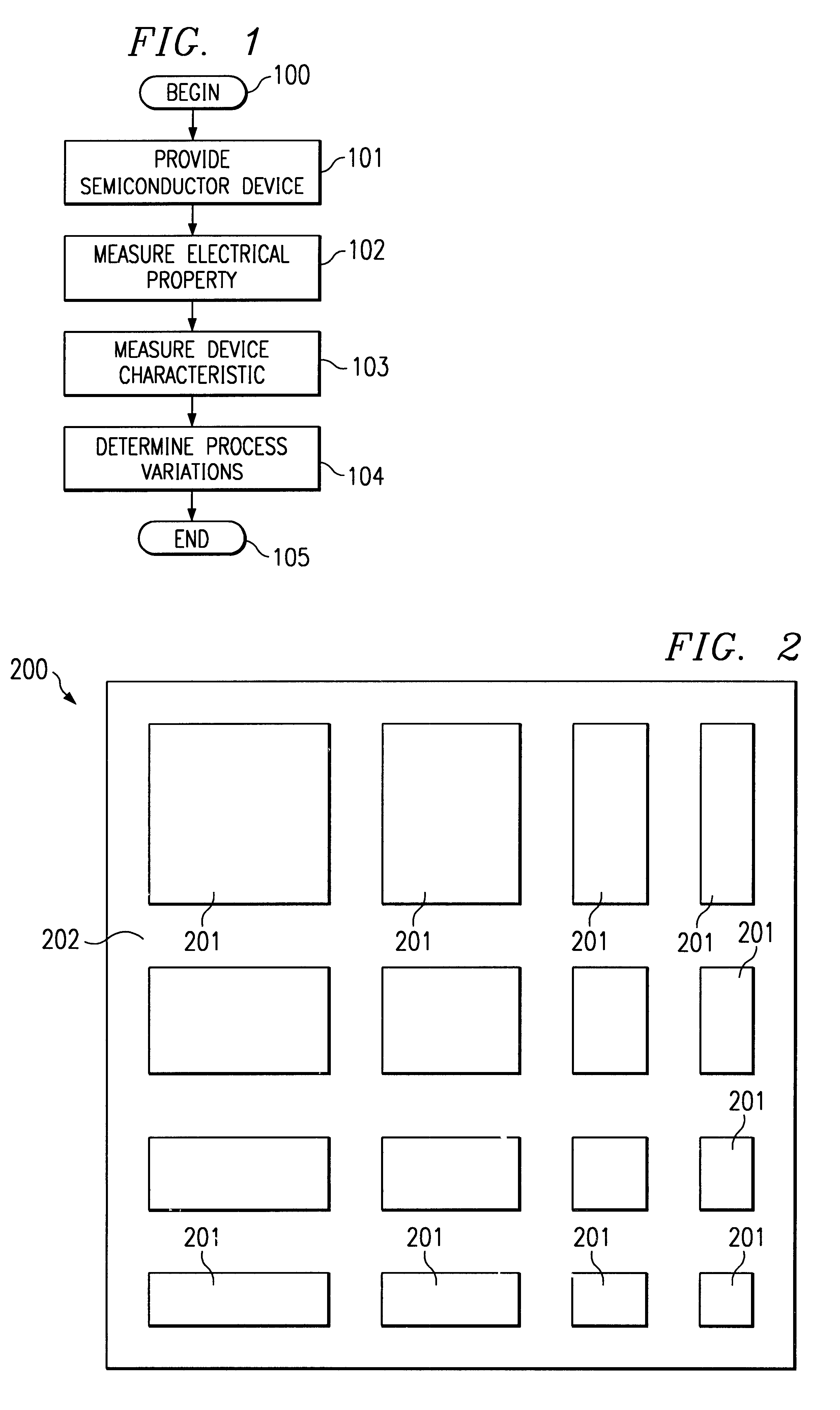
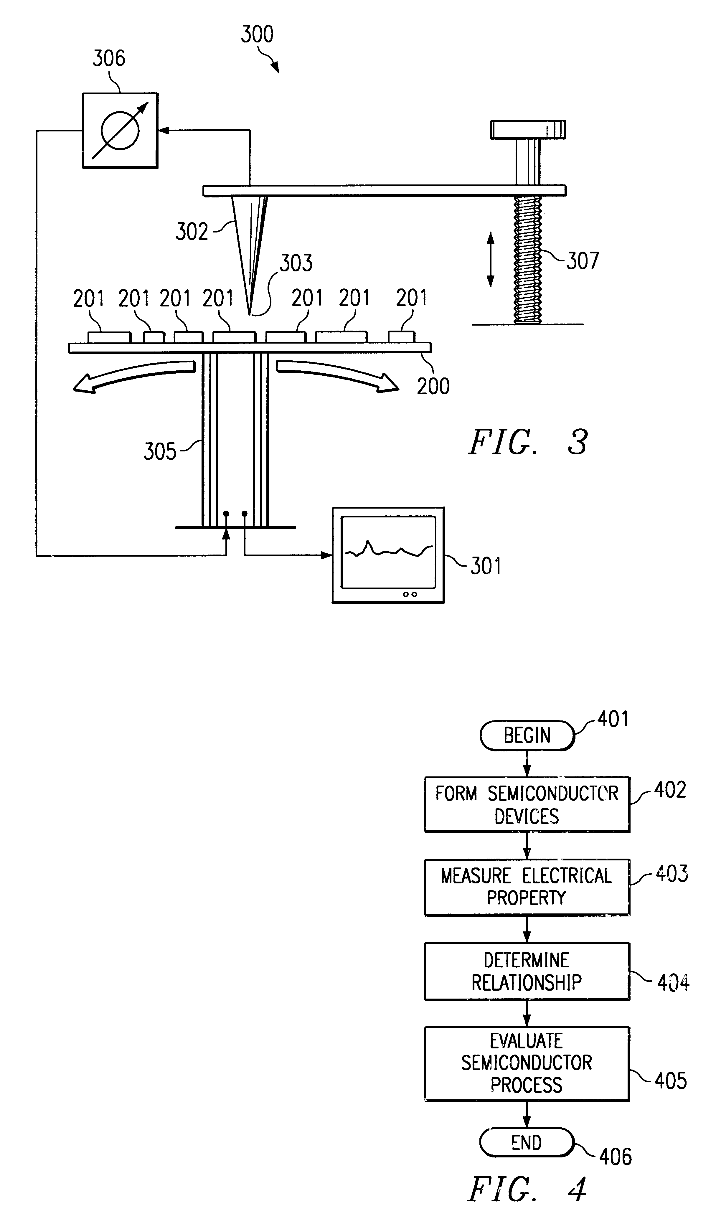
Referring to FIG. 1, an illustration of a flow diagram of one embodiment of a method for evaluating semiconductor devices and associated fabrication process is shown. The method begins at step 100. At step 101 a semiconductor device is provided having at least one selected geometric dimension. The semiconductor device may be created using advanced semiconductor processes and in one embodiment includes an array of capacitive structures fabricated to a minimum design rule. The geometric dimensions of the semiconductor devices are varied to separate an edge effect from a bulk effect. An edge effect typically includes a measured property that is impacted by the close proximity of the device boundary which may cause, among other things, electric field spreading, trap states, lattice defects or other defects. A bulk effect may include the situation in which the measured property is independent of any boundary effects. In one embodiment, the semiconductor device may include submicron geome...


PUM


Abstract

An apparatus and method for evaluating semiconductor structures and devices are provided. A method for evaluating at least one selected electrical property of a semiconductor device (201) in relation to a selected geometric dimension of the semiconductor device (201). The method further includes forming a plurality of semiconductor devices (201) on a substrate (202), the devices (201) having at least one geometric dimension, measuring the at least one electrical property of at least one of the semiconductor devices (201) using a scanning probe microscopy based technique, and determining a relationship between the measured electrical property and the selected geometric dimension of the semiconductor device (201). The method further includes evaluating at least one semiconductor fabrication process based upon the determined relationship.

Description

TECHNICAL FIELD OF THE INVENTIONThis invention generally relates to the field of electronic devices. More specifically this invention relates to an apparatus and method for evaluating semiconductor structures and devices.BACKGROUND OF THE INVENTIONAdvancements in the semiconductor industry have converged on developing submicron geometric devices for microelectronic circuits. Semiconductor fabrication processes, in their infancy, were sometimes plagued with fatal defectivity that inhibited the production of integrated circuits. As semiconductor fabrication processes became more advanced, the level and occurrence of defects in semiconductor devices have decreased. However, the reduction of semiconductor geometries to submicron levels has manifested inherent defect modes which may impact the performance of resulting semiconductor devices.Silicon wafers provide a common substrate used to fabricate multiple semiconductor devices. As geometries for semiconductor devices are reduced, the i...

Claims


Application Information

Patent Timeline
Patent Type & Authority Patents(United States)
IPC IPC(8): G01R31/303G01R31/28G01R31/312
CPCG01R31/303G01R31/312Y10S977/852
Inventor EDWARDS, HENRY L.MOISE, THEODORE S.WILK, GLEN D.
Owner TEXAS INSTR INC
Why Eureka
Try Eureka