Storage pixel sensor and array with compression

a pixel sensor and array technology, applied in the field of compression cmos image sensors and image sensor arrays, can solve the problem of limit the dynamic range of images that can be captured by the array

Inactive Publication Date: 2003-01-28
FOVEON
View PDF57 Cites 228 Cited by
  • Summary
  • Abstract
  • Description
  • Claims
  • Application Information

AI Technical Summary

Problems solved by technology

A problem encountered with prior-art imagers is a limitation on

Method used


Image

  • Storage pixel sensor and array with compression
  • Storage pixel sensor and array with compression
  • Storage pixel sensor and array with compression

Examples


first embodiment

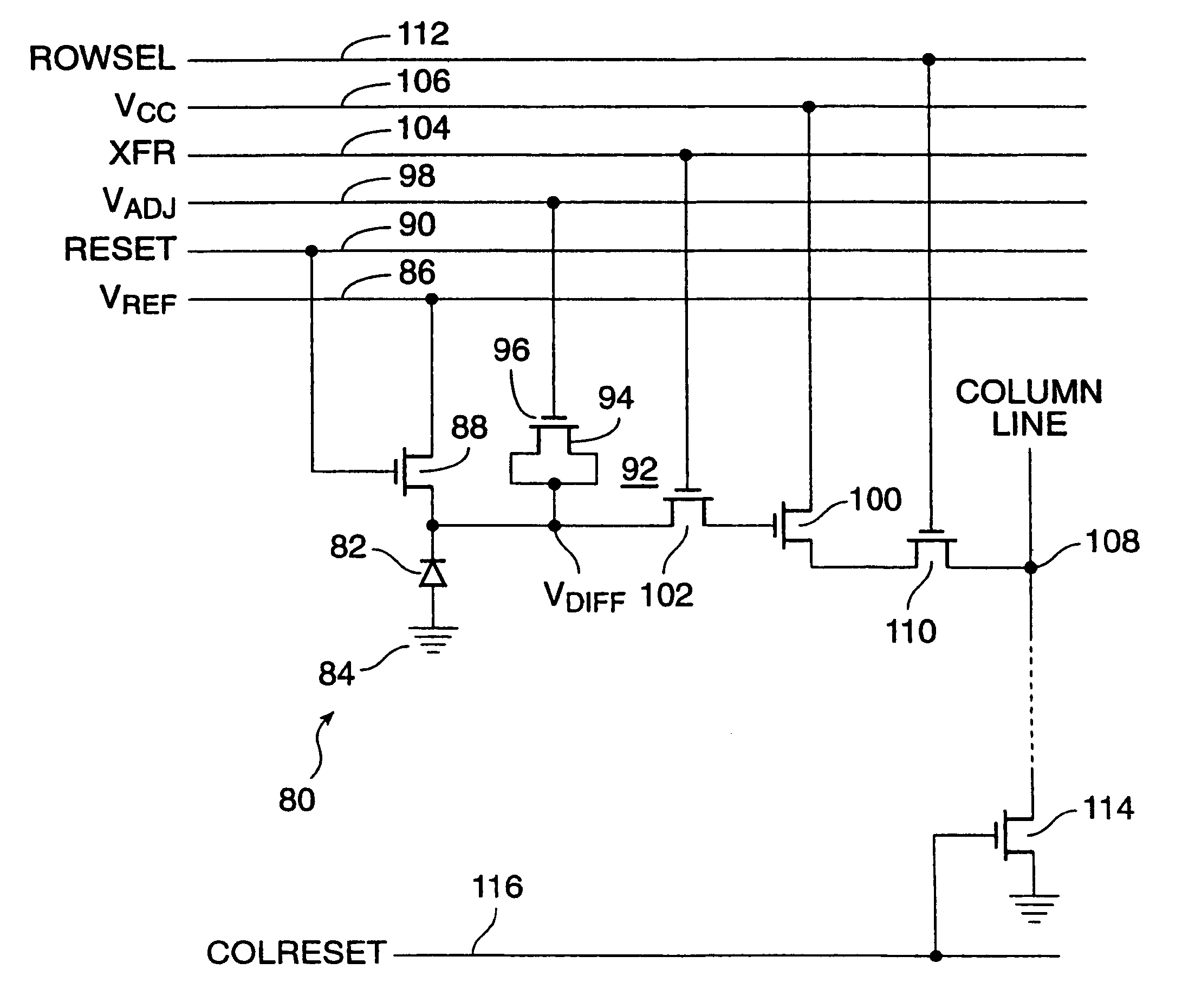
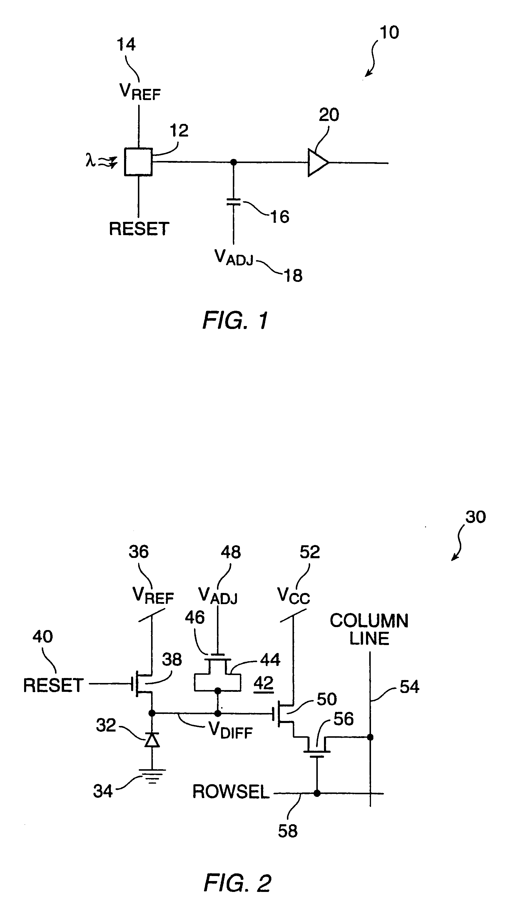
Referring now to FIG. 5, a schematic diagram illustrates a storage pixel 80 with intensity compression according to the present invention. FIG. 5 shows pixel 80 in the environment of an array of such pixels. Storage pixel sensor 80 comprises a photodiode 82 having its anode coupled to a fixed voltage potential 84 (shown in FIG. 5 as ground). The cathode of photodiode 82 connectable to a reference potential Vref 86 via a reset switch 88, shown in FIG. 5 as an N-Channel MOS transistor, so that the photodiode 82 is reverse biased. The gate of the N-Channel MOS transistor forming reset switch 88 is driven by a RESET signal on Reset line 90.

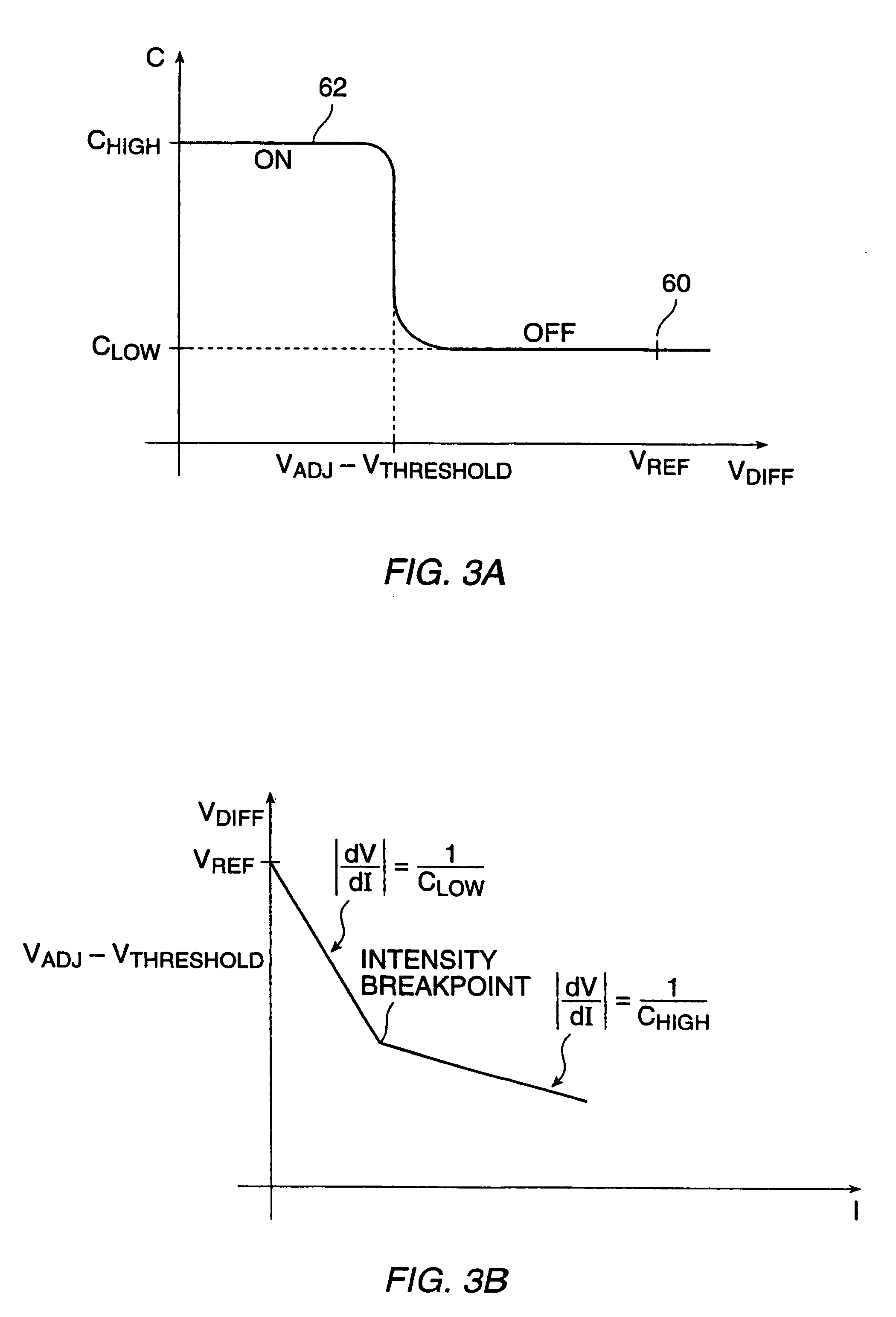
The cathode of photodiode 82 is also coupled to a nonlinear capacitor. The nonlinear capacitor has a compressive photocharge-to-voltage gain function. According to a presently preferred embodiment of the invention, the nonlinear capacitor comprises an MOS storage capacitor 92 having a first plate 94 comprising a channel region with a diffusion termina...

second embodiment

Referring now to FIG. 6, a storage pixel sensor 120 according to the present invention is depicted in a schematic diagram. As with the storage pixel sensor 80 of FIG. 5, storage pixel sensor 120 of FIG. 6 comprises a photodiode 122 having its anode coupled to a fixed voltage potential 124 (shown in FIG. 6 as ground). The cathode of photodiode 122 is coupled to a reference potential Vref 126 via a reset switch 128, shown in FIG. 6 as an N-Channel MOS transistor, so that the photodiode 122 is reverse biased. The gate of the N-Channel MOS transistor forming reset switch 128 is driven by a RESET line 130. The cathode of photodiode 122 is also connectable to a nonlinear capacitor 132, shown as an N-Channel MOS capacitor in FIG. 6, through a transfer switch 134, shown in FIG. 6 as an N-Channel MOS transistor. The gate of transfer switch 134 is driven by a XFR signal on transfer line 136. In this embodiment, the nonlinear capacitor is referred to as a storage capacitor, since it stores the...


PUM


Abstract

A storage pixel sensor disposed on a semiconductor substrate comprises a photosensor. At least one nonlinear capacitive element is coupled to the photosensor. At least one nonlinear capacitive element is arranged to have a compressive photocharge-to-voltage gain function. An amplifier has an input coupled to the nonlinear capacitor and an output. Other, non-capacitive elements may be employed to produce a compressive photo-charge-to-voltage gain having at least one breakpoint.

Description

1. Field of the InventionThe present invention relates to image sensors and arrays of image sensors. More particularly, the present invention relates to compressive CMOS image sensors and image sensor arrays for still camera and other applications and to methods for operating those arrays.2. The Prior ArtIntegrated image sensors are known in the art. Such sensors have been fabricated from charge-coupled devices (CCDs) and as bipolar and MOS image sensors.A problem encountered with prior-art imagers is a limitation on the dynamic range of images that can be captured by the array. Images that contain both low-light-level pixels and high-light-level pixels could be improved if the dynamic range of the imager could be increased.In an active pixel sensor, the sensitivity of measuring charges generated by photons can be described as a charge-to-voltage gain. Typically, in a prior art active pixel sensor, the charge-to-voltage gain is accounted for by two factors. A first factor is the rec...

Claims


Application Information

Patent Timeline
IPC IPC(8): H01L27/146H01L27/144H04N3/15H04N5/355H04N5/374H04N5/3745
CPCH01L27/1443H01L27/14609H04N5/37452H04N5/35527H04N5/374H04N25/575H04N25/59H04N25/771H04N25/76
Inventor MERRILL, RICHARD B.LYON, RICHARD F.
Owner FOVEON
Why Eureka
Try Eureka