Capacitive two dimensional sensor

a two-dimensional sensor and capacitive technology, applied in the field of capacitive two-dimensional sensors, can solve the problems of difficult production difficult to produce with a high yield of good devices, and high manufacturing cost of semiconductor chips of this size, so as to reduce residual signals and reduce residual signals

Inactive Publication Date: 2003-02-25
SENTRONICS CORP
View PDF2 Cites 135 Cited by
  • Summary
  • Abstract
  • Description
  • Claims
  • Application Information

AI Technical Summary

Problems solved by technology

A semiconductor chip of this size is expensive to fabricate and difficult to produce with a high yield of good devices.
This approach is more complex mechanically and simpler electronically.
This characteristic signal changes due to spreading of the finger under pressure and to angular misalignment of the finger with the sensor providing unsatisfactory results.

Method used


Image

  • Capacitive two dimensional sensor
  • Capacitive two dimensional sensor
  • Capacitive two dimensional sensor

Examples


Embodiment Construction

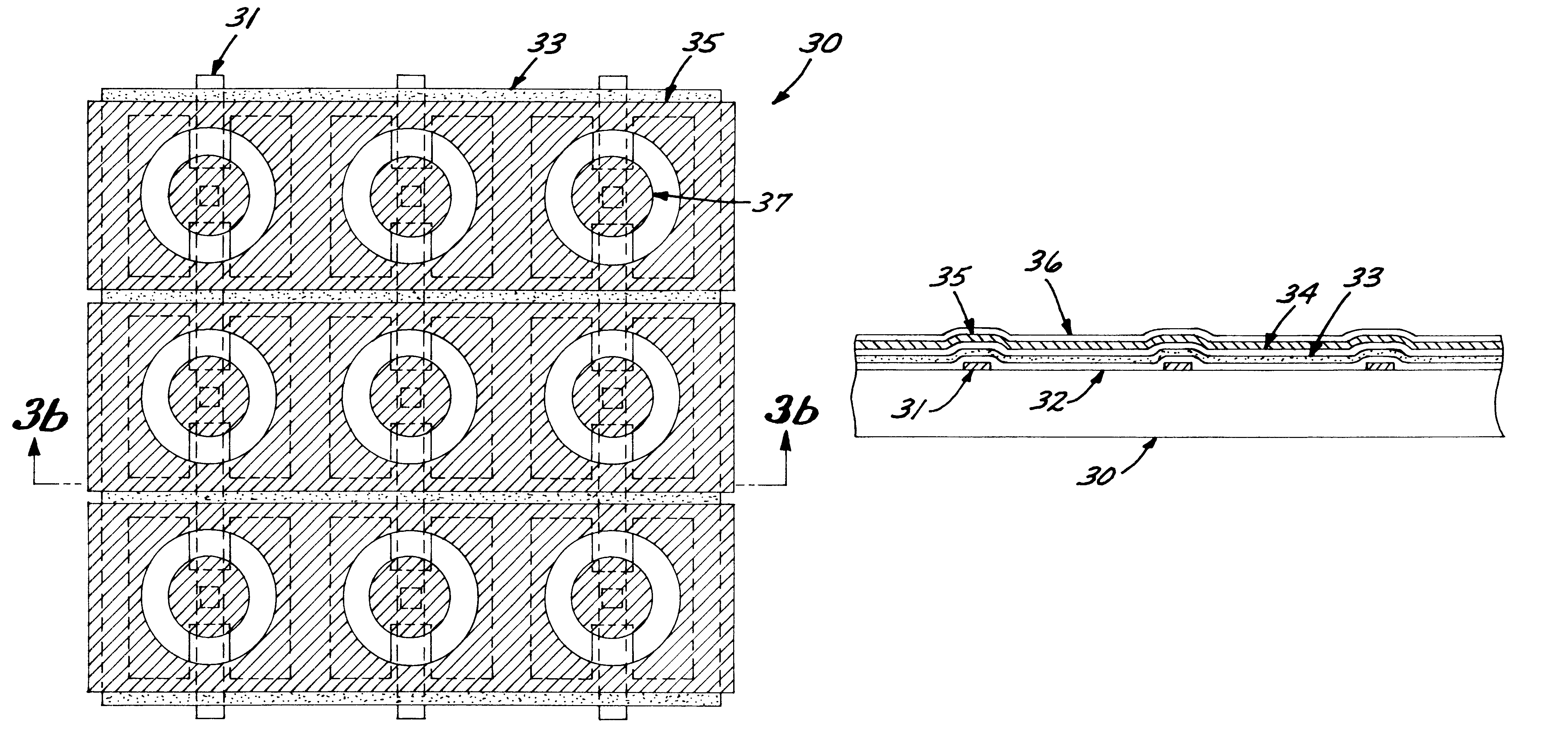
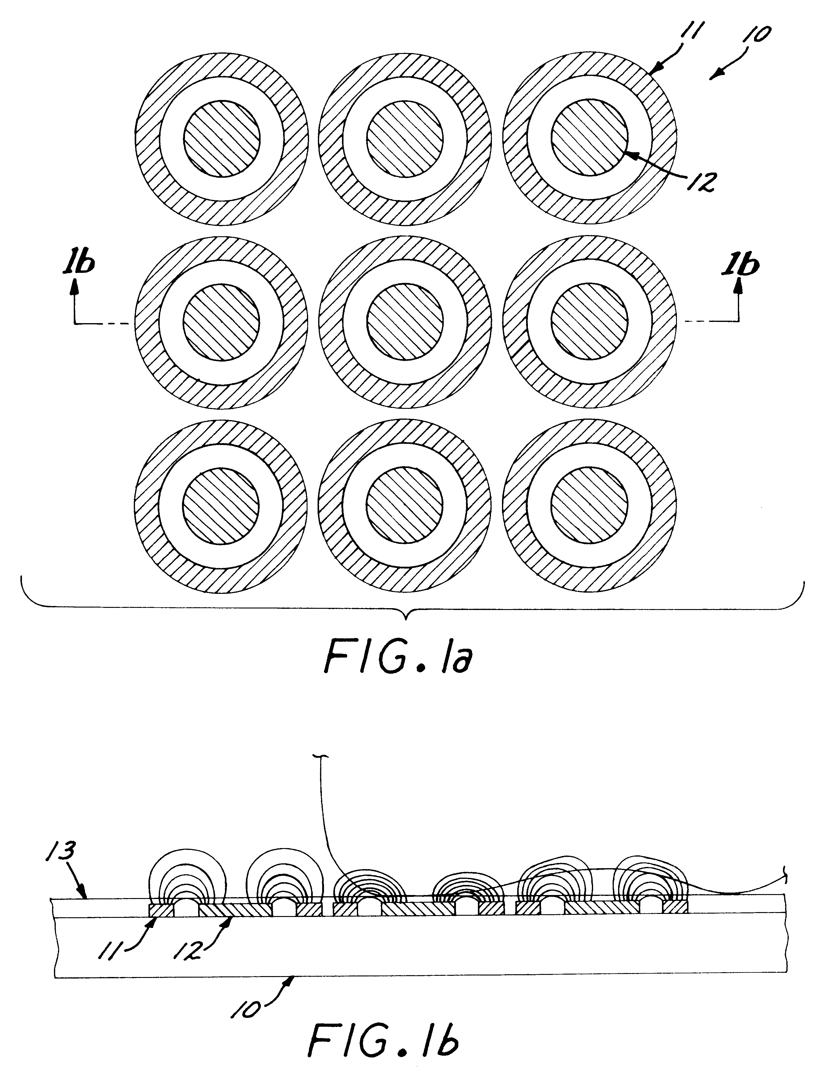
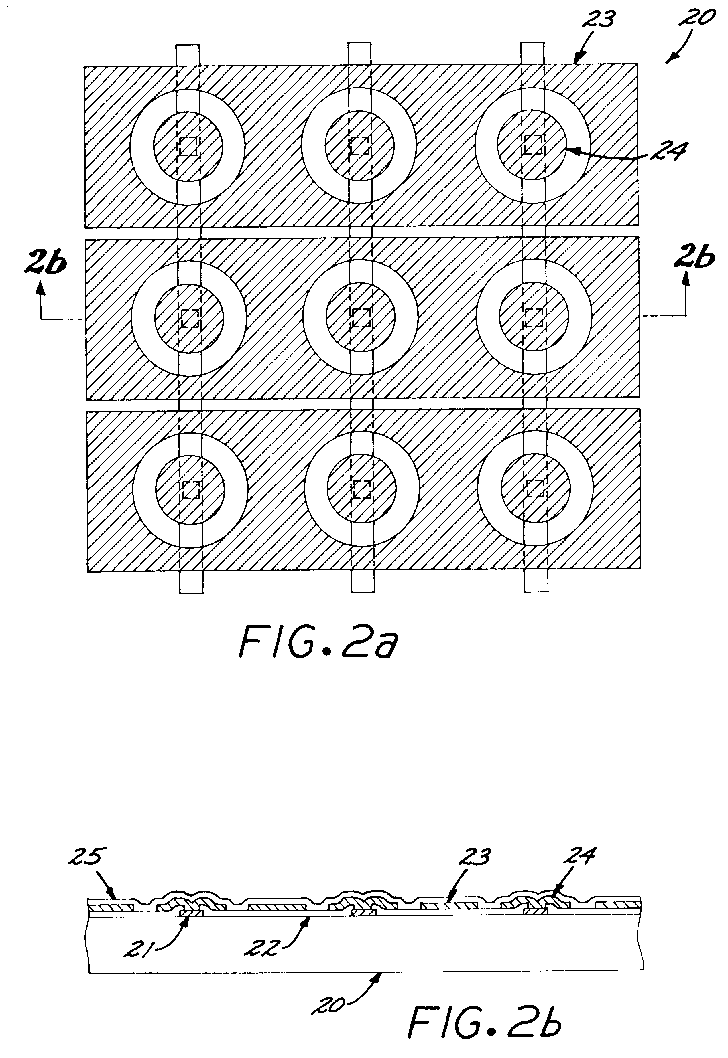
Referring to the figures, each element (pixel) in the sensor array of the present invention has drive and pickup electrodes, the drive electrodes and pickup electrodes not being required to be in a common plane or layer. Optionally, a shield electrode may also be used to provide isolation between drive signals and pick up signals and to control the distance above the surface that the array is sensitive to. The most sensitive area is the gap between the drive and pickup electrodes, the gap being ideally circular in shape to minimize the changes in sensitivity caused by the orientation of the fingerprint features (a square or rectangular gap will provide satisfactory results in most cases). Wider gaps will extend the sensitive area further above the array surface. A shield or other grounded conductors in the gap between the drive and pickup electrodes tends to move the sensitive area closer to the surface. It is preferable that the pickup electrode and the drive electrode are symmetri...


PUM


Abstract

A two dimensional array of electrods for sensing the presence or absence of the ridges in a fingerprint through capacitive measurements. Exciting signals are supplied from outside the array which allows the array to be fabricated from metal and insulator layers on non-semiconductor substrates such as glass or plastic using normal deposition and patterning techniques. A top protective layer consisting of hard, rigid material may be provided. The required electronic circuits are preferably located around the periphery of the array.

Description

1. Field of the InventionThe present invention relates to a new device using capacitance to detect fingerprint characteristics which is simpler and less expensive to fabricate than previous devices used for this purpose.2. Description of the Prior ArtPrevious capacitive fingerprint sensors have used arrays of electrodes with individual electronic circuits associated with each set of electrodes in the array. An element in the array may have one electrode, with the finger representing a grounded capacitor plate as described in U.S. Pat. No. 6,016,355 or it may have two electrodes with the finger representing a floating capacitor plate as described in another prior art device. In both cases, the change in capacitance due to a fingerprint feature is sensed by an individual electronic circuit located adjacent to or underneath the electrodes. The output of these individual circuits are electronically multiplexed together to form an image of the fingerprint.The electronic circuits must be ...

Claims


Application Information

Patent Timeline
Patent Type & Authority Patents(United States)
IPC IPC(8): G01D5/12G01D5/24G06K9/00
CPCG06K9/0002G01D5/2405G06V40/1306
Inventor HAYES, ROBERT S.
Owner SENTRONICS CORP
Why Eureka
Try Eureka