Electronic device and driving method

a driving method and electronic device technology, applied in semiconductor devices, electrical devices, instruments, etc., can solve the problems of increased wiring length, insufficient write in time and dispersion of electric current supplied, and burden on the screen to be larger

Inactive Publication Date: 2003-03-04
SEMICON ENERGY LAB CO LTD
View PDF6 Cites 110 Cited by
  • Summary
  • Abstract
  • Description
  • Claims
  • Application Information

AI Technical Summary

Problems solved by technology

However, the increase in the length of wirings which accompanies making larger screens becomes a cause of problems such as insufficient write in time and dispersion in the electric current supplied.
In particular, the dispersion in the amount of electric current supplied to the EL element due to the resistance of the electric current supply lines is directly connected with display irregularities such as uneven brightness within the screen and crosstalk, and therefore is a burden to making screens larger.
However, simply increasing the number of wirings in the pixel portion or increasing the cross sectional area of the wirings invites a reduction in the aperture ratio, and cannot be said to be a desirable method.

Method used


Image

  • Electronic device and driving method
  • Electronic device and driving method
  • Electronic device and driving method

Examples


embodiment 1

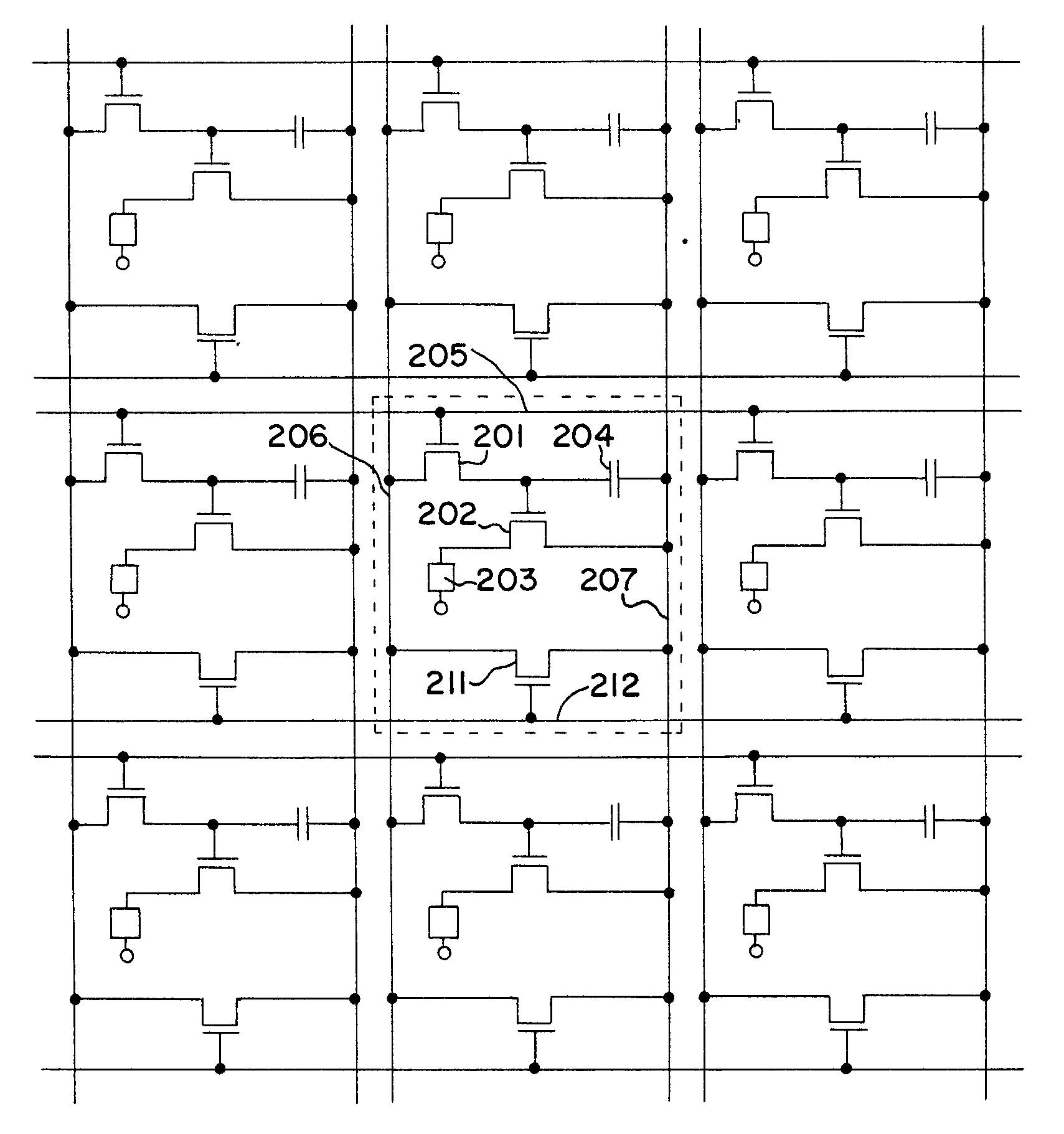
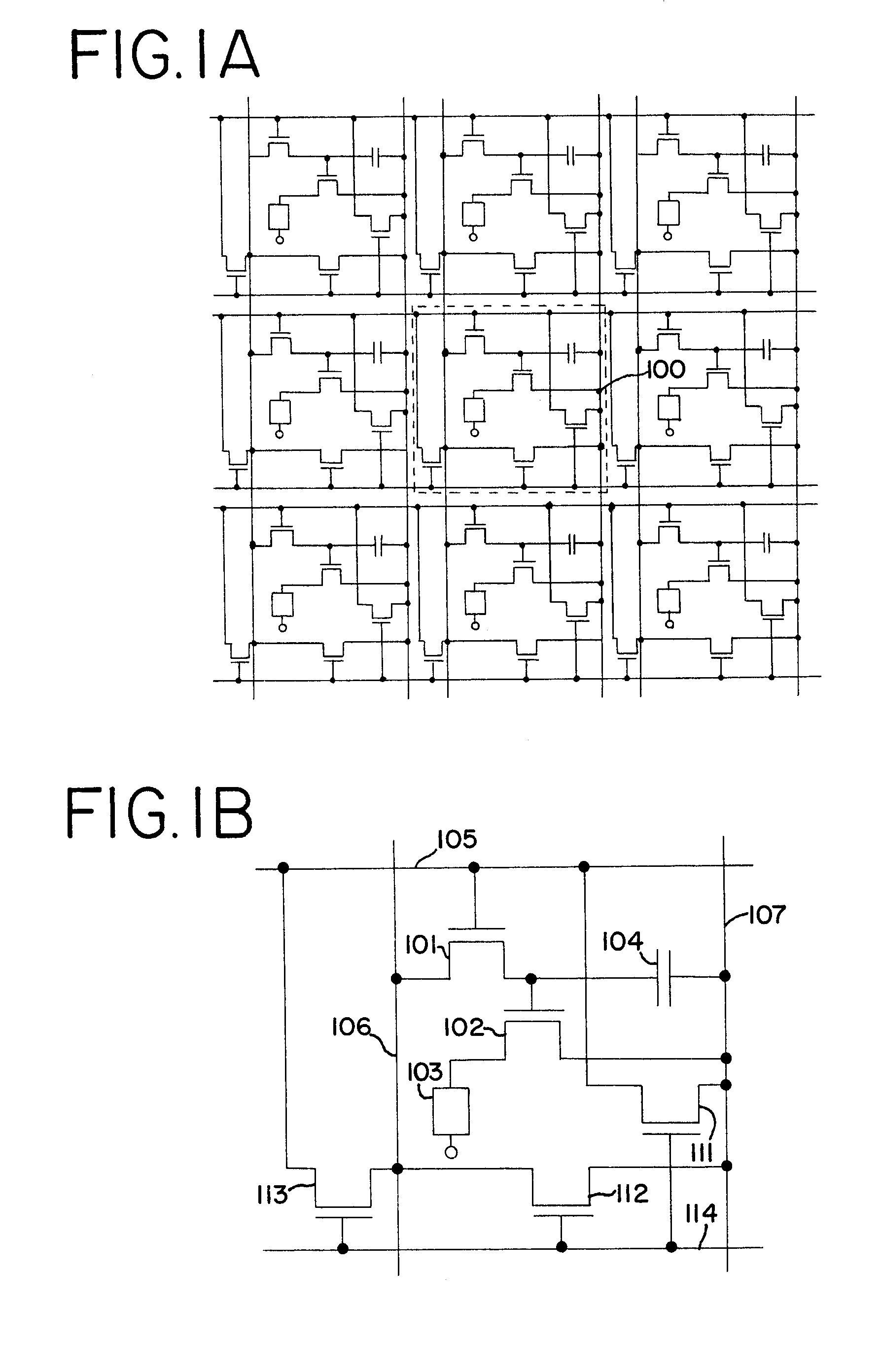
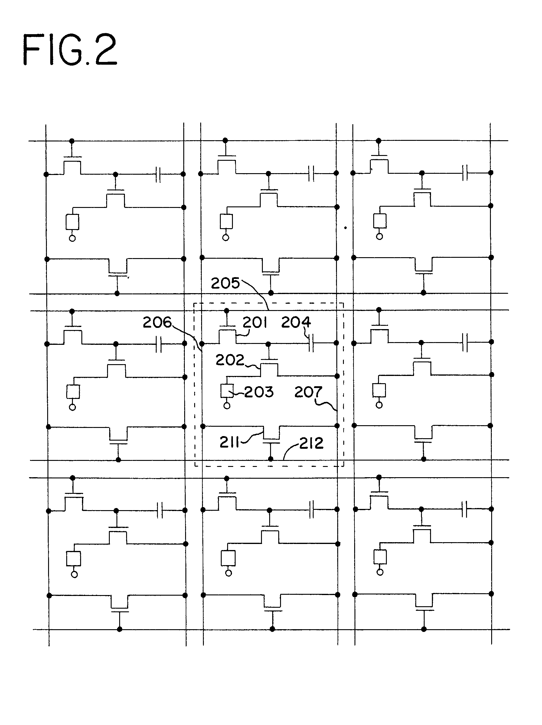
FIGS. 2 to 7 show examples of structures of circuits in a pixel portion in order to implement a structure of the present invention. One pixel surrounded by a dotted line frame with the figures is taken as a standard for the following discussion.

A source signal line 206 and an electric current supply line 207 are connected through a connection TFT 211 within a pixel in FIG. 2. In FIG. 3, an electric current supply line 308 and a source signal line 307 of an adjacent pixel are connected through a connection TFT 312. In this case, it becomes possible to avoid a large reduction in the aperture ratio, compared with FIG. 2, because the connection TFT can be arranged between two pixels. In FIG. 4, an electric current supply line 408 and a source signal line 406 are connected through a connection TFT 412 within the pixel itself, and in addition, are also connected to a source signal line 407, which is connected to an adjacent pixel, through a connection TFT 413. The electric current supply ...

embodiment 2

In Embodiment 2, the active layer of the n-channel TFT contains a source region, a drain region, a GOLD region, an LDD region, and a channel forming region, and the GOLD region overlaps with the gate electrode through the gate insulating film.

Further, there is not much need to worry about degradation due to hot carrier injection with the p-channel TFT of the CMOS circuit, and therefore LDD regions need not be formed in particular. It is of course possible to form an LDD region similar to that of the n-channel TFT, as a measure against hot carriers.

In addition, when using a CMOS circuit in which electric current flows in both directions in the channel forming region, namely a CMOS circuit in which the roles of the source region and the drain region interchange, it is preferable that LDD regions be formed on both sides of the channel forming region of the n-channel TFT forming the CMOS circuit, sandwiching the channel forming region. A circuit such as a transmission gate used in dot-s...

embodiment 3

An example of manufacturing an electronic device using the present invention is explained in Embodiment 3.

FIG. 14A is a top view of an electronic device using the present invention and FIG. 14B shows a cross sectional diagram in which FIG. 14A is cut along the line X-X'. In FIG. 14A, reference numeral 4001 is a substrate, reference numeral 4002 is a pixel portion, reference numeral 4003 is a source signal line side driver circuit, and reference numeral 4004 is a gate signal line side driver circuit. The respective driver circuits are connected to external equipments, through an FPC 4008, via wirings 4005, 4006 and 4007.

A covering material 4009, an airtight sealing material 4010 and a sealing material (also referred to as a housing material) 4011 (shown in FIG. 14B) are formed so as to enclose the pixel portion, preferably the driver circuits and the pixel portion, at this point.

Further, FIG. 14B is a cross sectional structure of the electronic device of Embodiment 3. A driver circui...


PUM


Abstract

An electro-optical device is provided having a pixel portion with a novel structure, and in which display irregularities such as crosstalk, which develop due to a drop in voltage caused by the wiring resistance of electric current supply lines in an electro-optical device, are improved upon. Attention is drawn to the fact that during a period in which write in of a signal to a pixel from a signal line is not performed, a signal is not input to a source signal line and to a gate signal line, but are at a fixed electric potential. An electric current supply line and a source signal line, or an electric current supply line and a gate signal line, are connected through a switching transistor. A signal is input to a connection control line during a sustain period, and the connection transistor is made conductive. The source signal line or the gate signal line is therefore utilized as a pathway for supplying electric current to the EL element.

Description

1. Field of the InventionThe present invention relates to a structure of an electronic device. In particular, the present invention relates to an active matrix electronic device having a thin film transistor (TFT) formed on an insulating body.2. Description of the Related ArtFlat panel displays have been drawing attention in recent years as substitutes for LCDs (liquid crystal displays), and research into such displays is proceeding apace.LCDs can roughly be divided into two types of driving methods. One is a passive matrix type using an LCD such as an STN-LCD, and the other is an active matrix type using an LCD such as a TFT-LCD. EL displays can also be similarly broken down roughly into two types; one a passive type, and the other an active type.For the passive type, wirings which become electrodes are arranged in portions above and below EL elements. Voltages are applied to the wirings in order, and the EL elements turn on due to the flow of an electric current. On the other hand...

Claims


Application Information

Patent Timeline
Patent Type & Authority Patents(United States)
IPC IPC(8): G09G3/32G09G3/30G09G3/20H01L27/32
CPCG09G3/3233G09G3/3258G09G3/2022H01L51/5237G09G2300/0408G09G2300/0426G09G2300/0465G09G2300/0809G09G2300/0814G09G2300/0842G09G2300/0861G09G2320/0204G09G2320/0209G09G2320/0214G09G2320/0223G09G2320/0233H01L27/3244G09G3/30H10K59/12H10K50/8428H10K50/846H10K50/8426H10K50/844
Inventor KIMURA, HAJIME
Owner SEMICON ENERGY LAB CO LTD
Why Eureka
Try Eureka