Apparatus and method for depositing superior Ta(N)/copper thin films for barrier and seed applications in semiconductor processing

Inactive Publication Date: 2003-04-01
NOVELLUS SYSTEMS
View PDF18 Cites 14 Cited by
  • Summary
  • Abstract
  • Description
  • Claims
  • Application Information

AI Technical Summary

Benefits of technology

is to provide a method of depositing a superior copper seed layer at sufficiently low temperatures so that the copper seed layer

Problems solved by technology

This barrier layer prevents diffusion of copper into the semiconductor devices as copper diffusion is detrimental to the performance of the devices resulting in shorts.
Standard PVD techniques are proven to be inadequate for depositing films in narrow, high aspect ratio structures with necessary and sufficient step coverage.
However, many of the IPVD sources suffer from the fact that they cannot produce a sufficiently high density plasma that can adequately ionize the depositing metal species.
Howe

Method used


Image

  • Apparatus and method for depositing superior Ta(N)/copper thin films for barrier and seed applications in semiconductor processing
  • Apparatus and method for depositing superior Ta(N)/copper thin films for barrier and seed applications in semiconductor processing
  • Apparatus and method for depositing superior Ta(N)/copper thin films for barrier and seed applications in semiconductor processing

Examples


Embodiment Construction

)

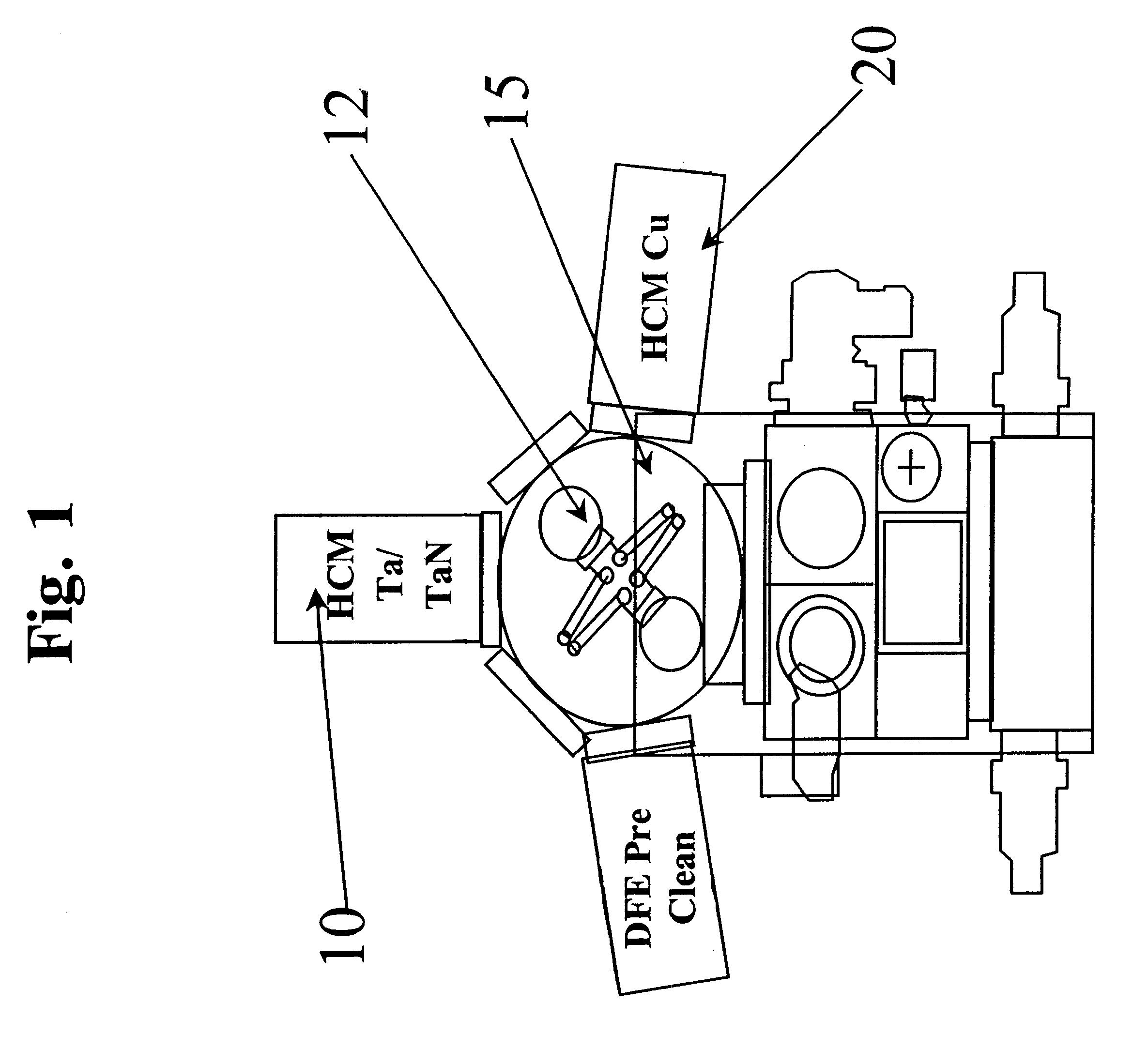
In describing the preferred embodiment of the present invention, reference will be made herein to FIGS. 1-5 of the drawings in which like numerals refer to like features of the invention. Features of the invention are not necessarily shown to scale in the drawings.

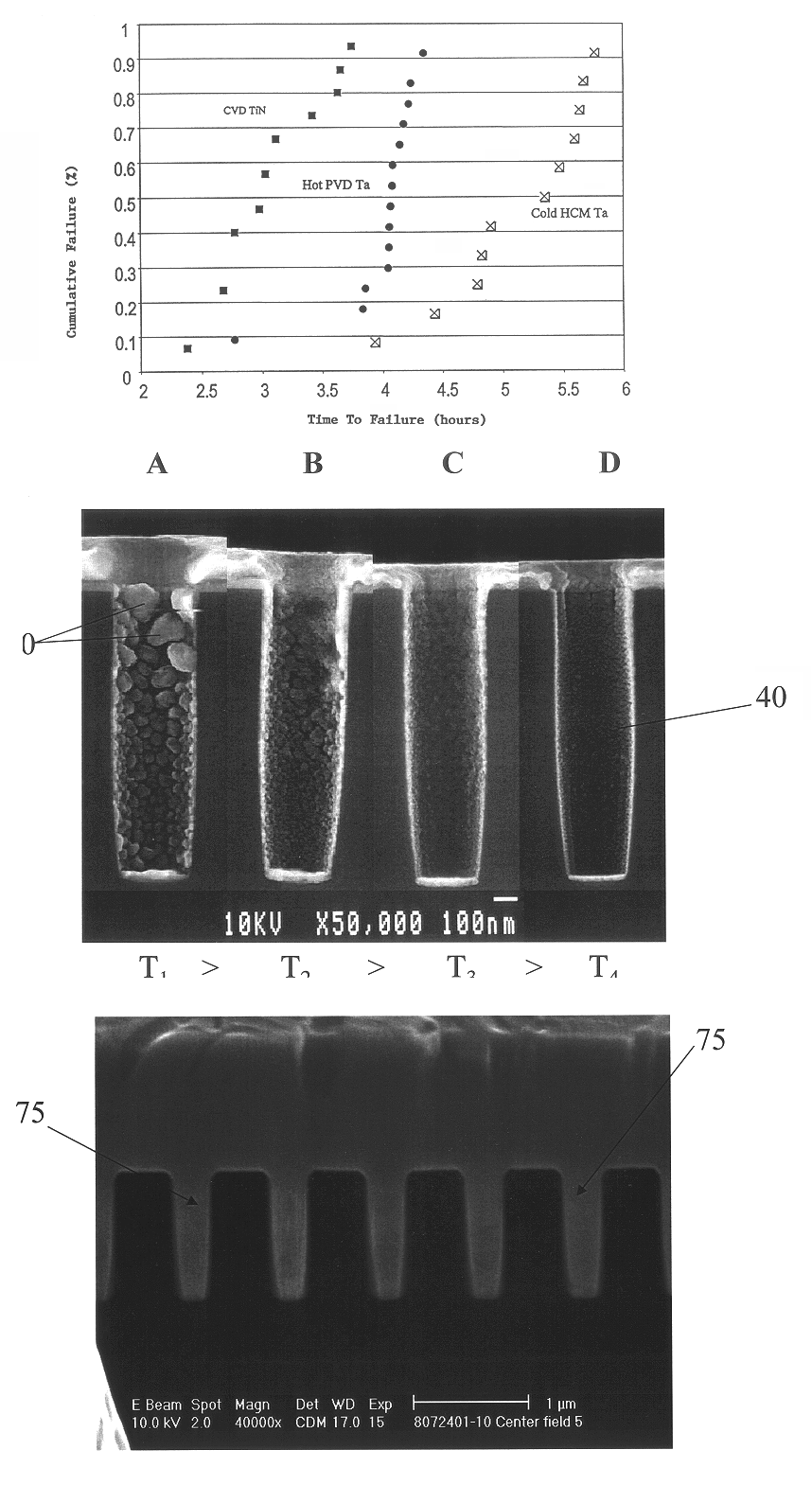
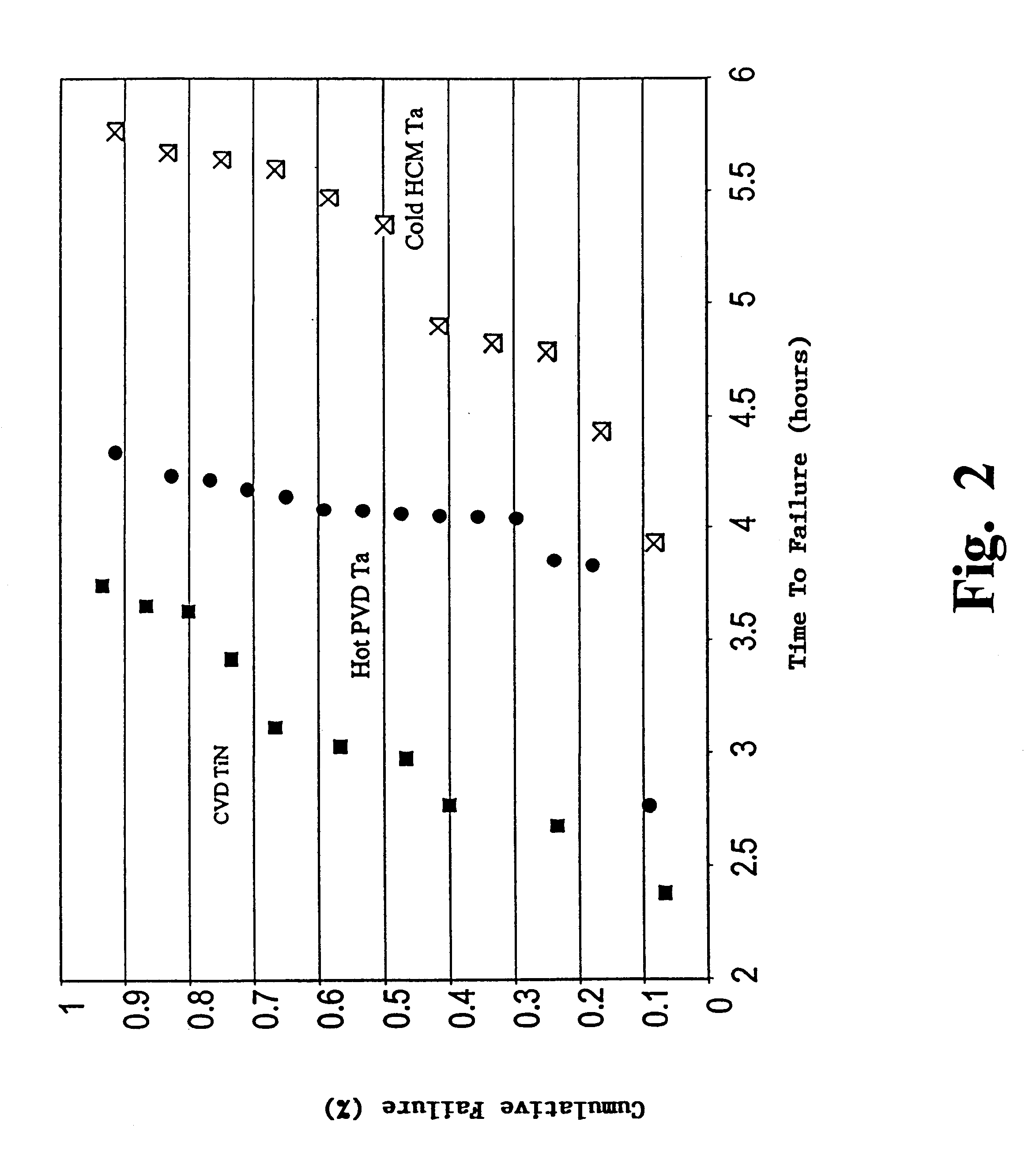
The present invention is directed to a method of depositing barrier films comprising tantalum, tantalum nitride and tantalum / tantalum nitride, and copper seed layers in high aspect ratio openings such as vias, contacts or trenches under low temperature conditions. The barrier films and seed layers of the present invention are deposited at extremely low temperatures wherein the wafer stage temperature of the sputter source is about -70.degree. C. to about 0.degree. C.; preferably about -50.degree. C., and the wafer is cooled to a temperature of about 20.degree. C. to about -10.degree. C. The resulting tantalum / tantalum nitride barrier films and copper seed layers are superior in surface smoothness, grain size and uniformit...


PUM


Abstract

A method of depositing thin films comprising tantalum, tantalum nitride, and copper for barrier films and seed layers within high aspect ratio openings used for copper interconnects. The barrier films and seed layers are deposited at extremely low temperature conditions wherein the wafer stage temperature of the sputter source is chilled to about -70° C. to about 0° C. Most preferably, the present invention is practiced using a hollow cathode magnetron. The resulting tantalum and/or tantalum nitride barrier films and copper seed layers are superior in surface smoothness, grain size and uniformity such that subsequent filling of the high aspect ratio opening is substantially void-free.

Description

1. Field of the InventionThe present invention relates to an apparatus and method for depositing tantalum (Ta) and tantalum nitride (TaN) barrier films, and copper (copper) thin films for applications in semiconductor processing. The preferred embodiment of this invention is related to U.S. Pat. No. 5,482,611 entitled "Physical Vapor Deposition Employing Ion Extraction From a Plasma" issued on Jan. 9, 1996 to Helmer et al., and assigned to the same assignee, Novellus Systems, Inc., and incorporated herein by reference in its entirety.2. Description of Related ArtTantalum and / or tantalum nitride for barrier liners and copper seed layers are being considered by all major manufacturers as the primary interconnect metals for applications in semiconductor processing in the next generation of integrated circuits (ICs). This is primarily due to lower manufacturing costs and increased performance of the ICs when copper is used as the primary interconnect metal as opposed to aluminum.In a ty...

Claims


Application Information

Patent Timeline
IPC IPC(8): H01L21/285H01L21/70H01L21/02H01L21/768
CPCH01L21/2855H01L21/76876H01L21/76873H01L21/76843
Inventor ASHTIANI, KAIHAN A.BIBERGER, MAXIMILIAN A.KLAWUHN, ERICH R.LAI, KWOK FAILEVY, KARL B.RYMER, J. PATRICK
Owner NOVELLUS SYSTEMS
Why Eureka
Try Eureka