Test and burn-in apparatus, in-line system using the test and burn-in apparatus, and test method using the in-line system

a test and burnin technology, applied in the direction of individual semiconductor device testing, semiconductor/solid-state device testing/measurement, instruments, etc., can solve the problems of time requirements, added time and complexity, and increased time and complexity

Inactive Publication Date: 2003-05-13
SAMSUNG ELECTRONICS CO LTD
View PDF7 Cites 89 Cited by
  • Summary
  • Abstract
  • Description
  • Claims
  • Application Information

AI Technical Summary

Benefits of technology

It is still another object of the present invention to provide an improved testing method which includes a burn-in process having a reduced number of steps, requires less time to perform, and uses equipment occupying less space.

Problems solved by technology

These general steps require time to perform.
The time requirements are even worse when rework is required following the main process.
Unfortunately, as indicated above, conventional testers require additional equipment for transporting between test steps and transferring between trays (handling) both the devices to be tested and those which have already been tested.
Furthermore, shifting the devices between trays during every test step adds time and complexity but does not add any value in the performance of the tests.
In fact, the conventional handling requirements add cost and complexity to the semiconductor device manufacturing process without any corresponding benefits.
Specifically, the prior art handlers increase significantly the space and time requirements for moving the devices through the back-end process, as well as the costs associated due to increased equipment requirements.
Also, semiconductor devices being manipulated by the handler are faced with the possibility of considerable damage during movement between trays.
Another significant problem in the prior art is that the current burn-in testers require a long test time.
The excessive test time is further compounded by the amount of time it takes to transfer the devices between the burn-in board and the device tray, the time it takes to load and unload the burn-in board, and the time it takes to raise or drop the test temperature and / or to check the burn-in process or signals.
Accordingly, all of the above-discussed testing steps--which are required for every semiconductor device--impose a heavy cost burden on the end-consumer.
Finally, typical burn-in testers perform at a slow test rate and a low test accuracy.
This testing technique makes it difficult to apply test signals to the specific device to be tested.
Furthermore, typical burn-in testers have a long serial scanning time when compared with normal testers.
Another major problem in the prior art involves the prior art retest procedures.
Using this type of retest adds to the time requirements and complexity of the back-end process.
As a consequence of all of these drawbacks, it is considerably difficult to systemize the back-end process of the in-line system.
Use of the prior art processes and equipment results in dropped productivity and lost cost-efficiency.

Method used


Image

  • Test and burn-in apparatus, in-line system using the test and burn-in apparatus, and test method using the in-line system
  • Test and burn-in apparatus, in-line system using the test and burn-in apparatus, and test method using the in-line system
  • Test and burn-in apparatus, in-line system using the test and burn-in apparatus, and test method using the in-line system

Examples


Embodiment Construction

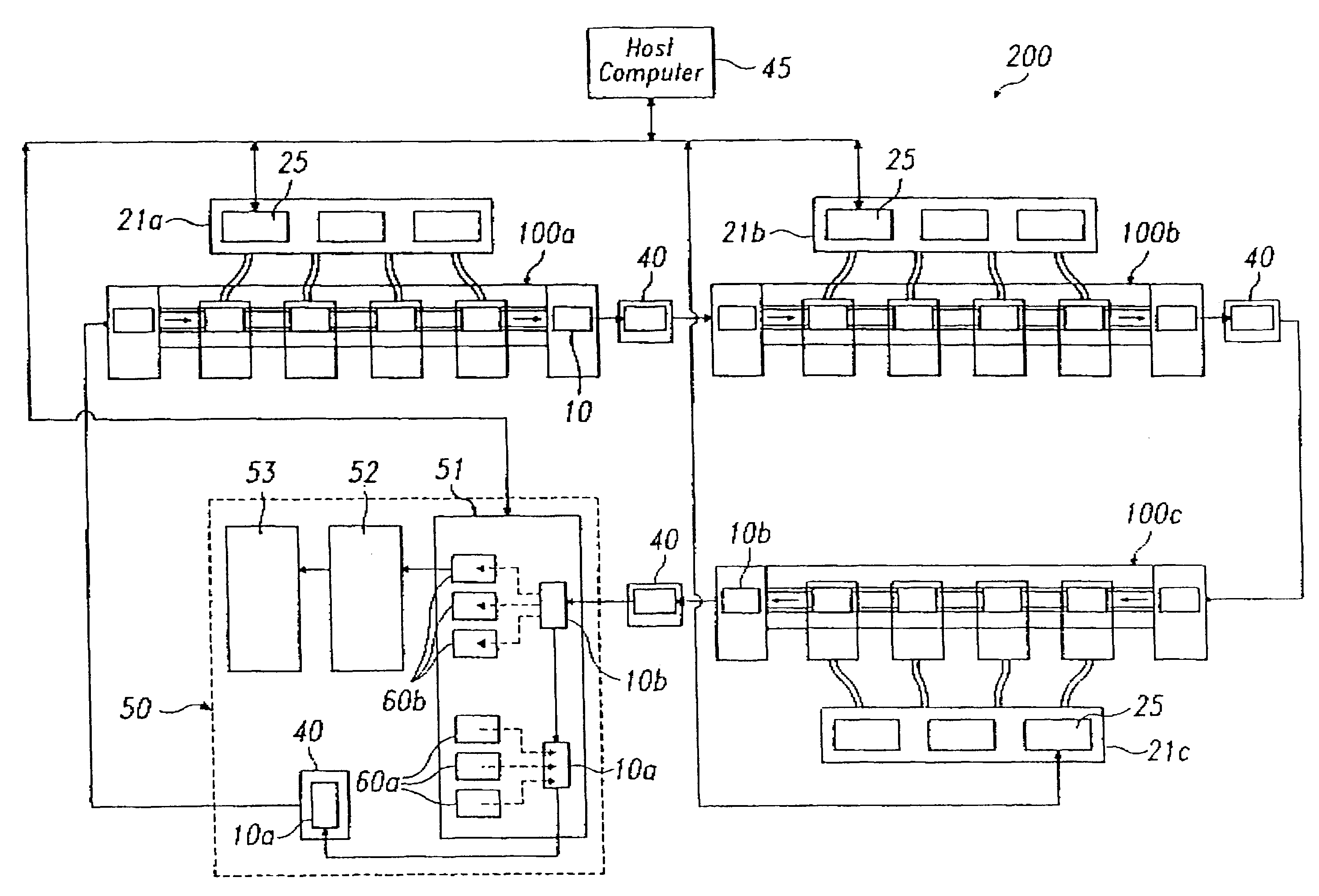
The preferred embodiments of the present invention will now be described more fully with reference to the accompanying drawings, in which like numerals represent like elements. It should be noted, however, that this invention may be embodied in many different forms and the claims should not be construed as being limited to the embodiments set forth in this description. Rather, these embodiments are provided by way of illustration only, so that the disclosure will be thorough and complete and convey the spirit but not scope of the invention to those skilled in the art. The scope is limited solely by the claims.

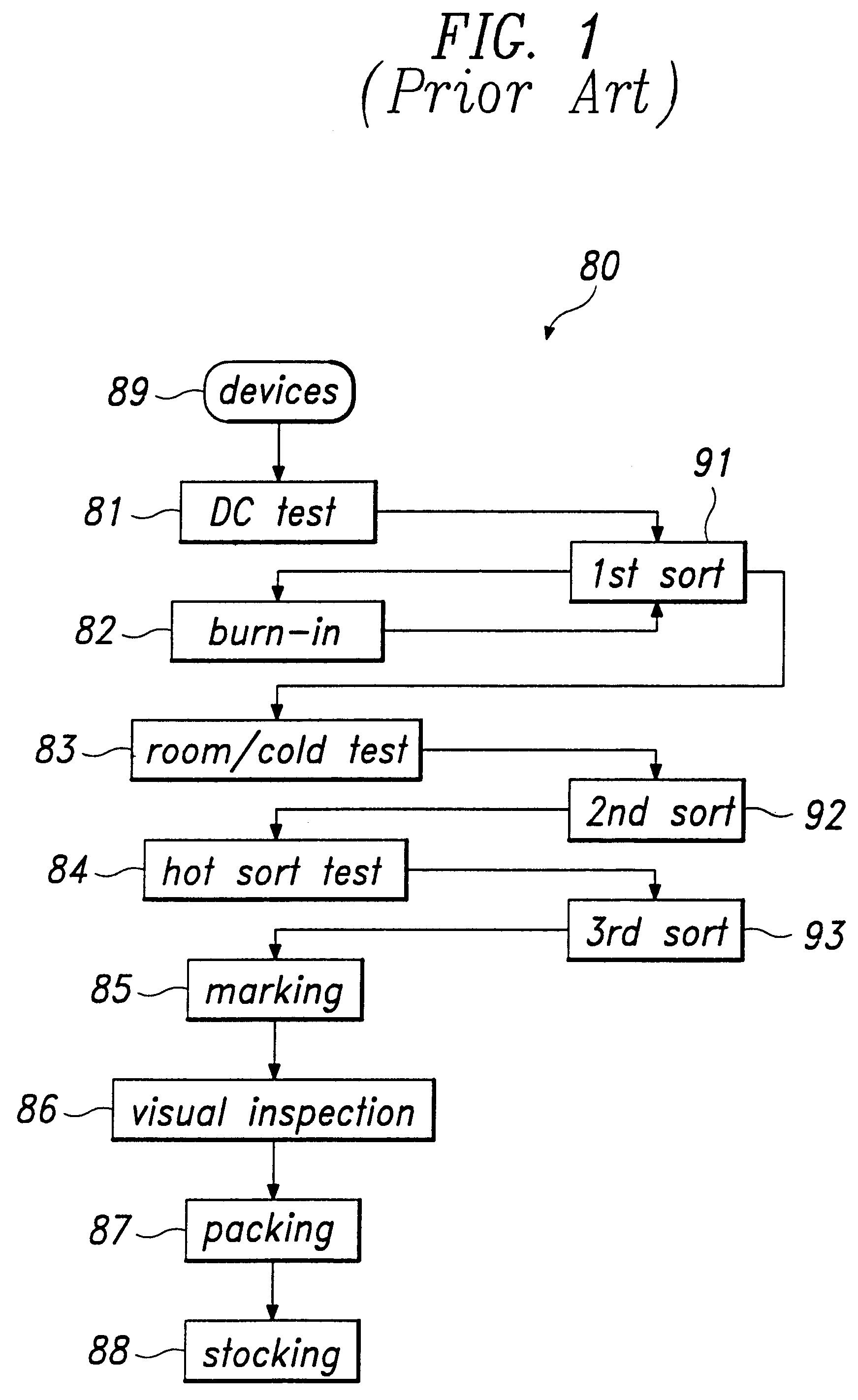
Various tests are required for ensuring the proper functioning of semiconductor devices. These tests are performed using one or more test and burn-in apparatuses in accordance with the present invention. In particular, the test and burn-in apparatuses (TABI) are so called because in the present invention, they enable a burn-in process in addition to the typical semiconductor de...


PUM


Abstract

An apparatus for testing semiconductor devices allows various testing processes, including a burn-in process, to be performed at the same testing stage. Test trays which contain the semiconductor devices are used throughout an in-line system so that an entire back-end process can be performed without loading / unloading the semiconductor devices between the various tests. The in-line system includes multiple test and burn-in apparatuses as well as a single sorting unit which performs a composite sorting operation after all the testing processes. A method for testing semiconductor devices in the in-line system includes testing the semiconductor devices in the test trays using the test and burn-in apparatus, transferring the test trays to a different testing apparatus for a second testing, and finally sorting the semiconductor devices after all testing processes have been performed based on a final sorting map created by combining test tray maps generated during each of the tests.

Description

This application is related to Korean patent application No. 97-12256 filed on Apr. 2, 1997 entitled "Method for Generating Lot in Semiconductor Test Process System" which is herein incorporated by reference for all purposes.1. Field of the InventionThe present invention relates generally to an apparatus and method for testing semiconductor devices. More particularly, the present invention relates to a test and burn-in apparatus for semiconductor chip package devices, an in-line system which includes the test and burn-in apparatus, and a test method which employs the in-line system.2. Description of the Related ArtA manufacturing process for producing semiconductor devices generally includes three sub-processes: a wafer fabrication process; a package assembly process; and a back-end process. The wafer fabrication process encompasses the procedures for creating a large number of circuits on a thin disc, or wafer, of semiconductor material such as silicon. The package assembly process...

Claims


Application Information

Patent Timeline
Patent Type & Authority Patents(United States)
IPC IPC(8): G01R1/02G01R1/04G01R31/28G01R31/26H01L21/66
CPCG01R31/2849G01R1/0408G01R31/28
Inventor MAENG, JU SEOK
Owner SAMSUNG ELECTRONICS CO LTD
Why Eureka
Try Eureka