Sealing structure for display device

Inactive Publication Date: 2003-07-08
SANYO ELECTRIC CO LTD
View PDF6 Cites 144 Cited by
  • Summary
  • Abstract
  • Description
  • Claims
  • Application Information

AI Technical Summary

Problems solved by technology

This light radiates outward through the side of the transparent anode via the transparent insulator substrate, resulting in light emission.
When, for example, a defect such as a pinhole is present in the counter electrode 6, moisture entering from the pinhole may cause oxidation of the counter electrode 6 or separation between the organic EL l

Method used


Image

  • Sealing structure for display device
  • Sealing structure for display device
  • Sealing structure for display device

Examples


Embodiment Construction

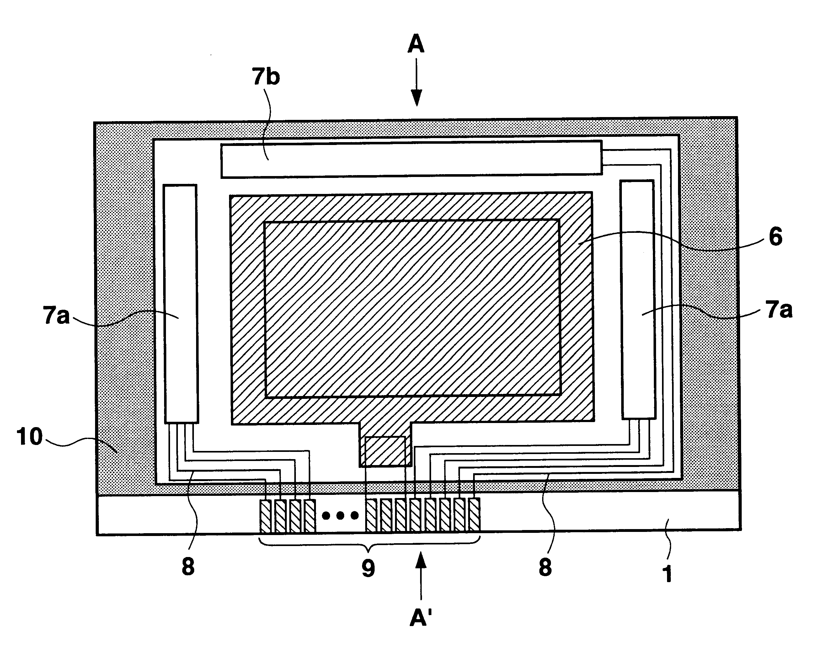
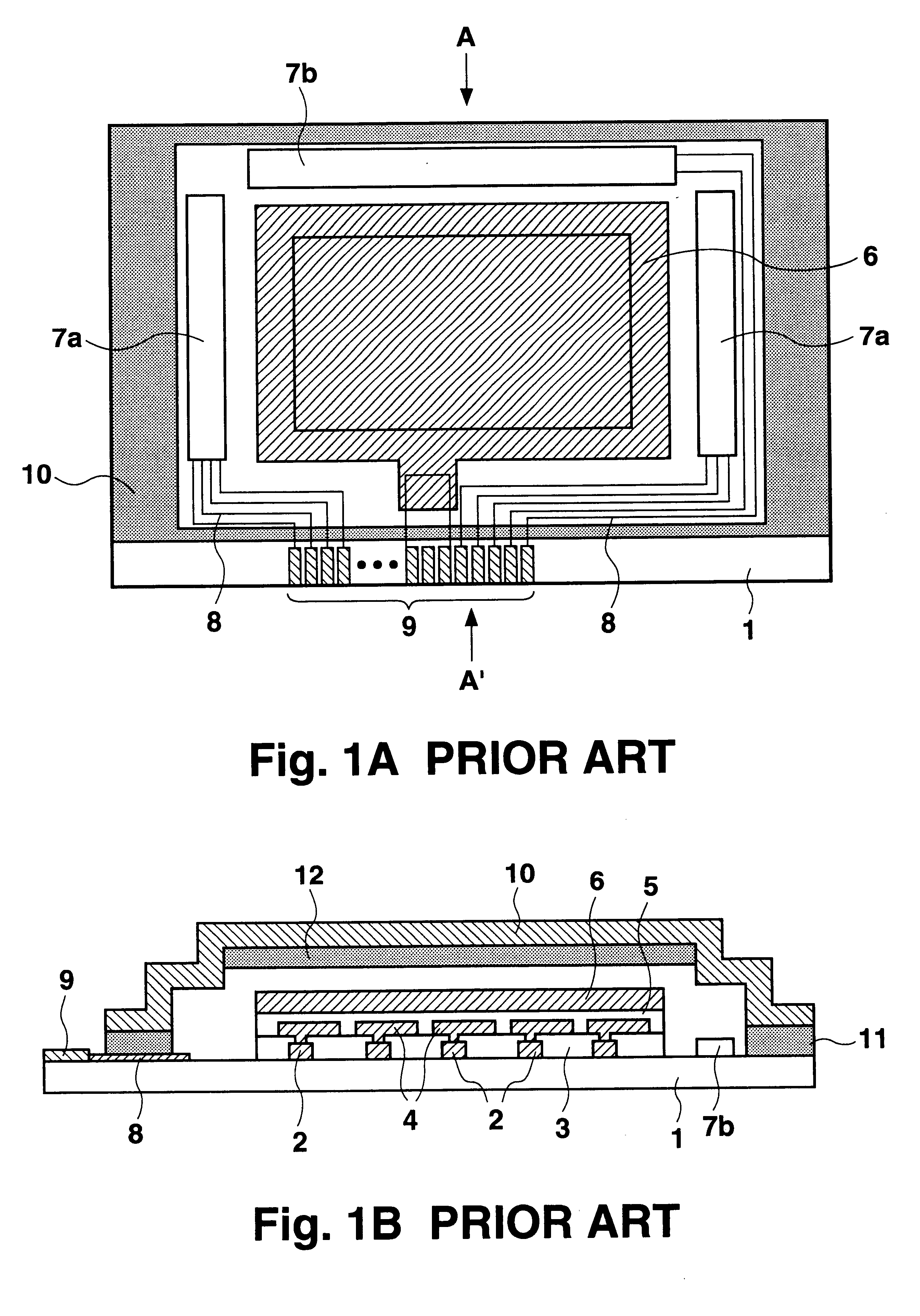
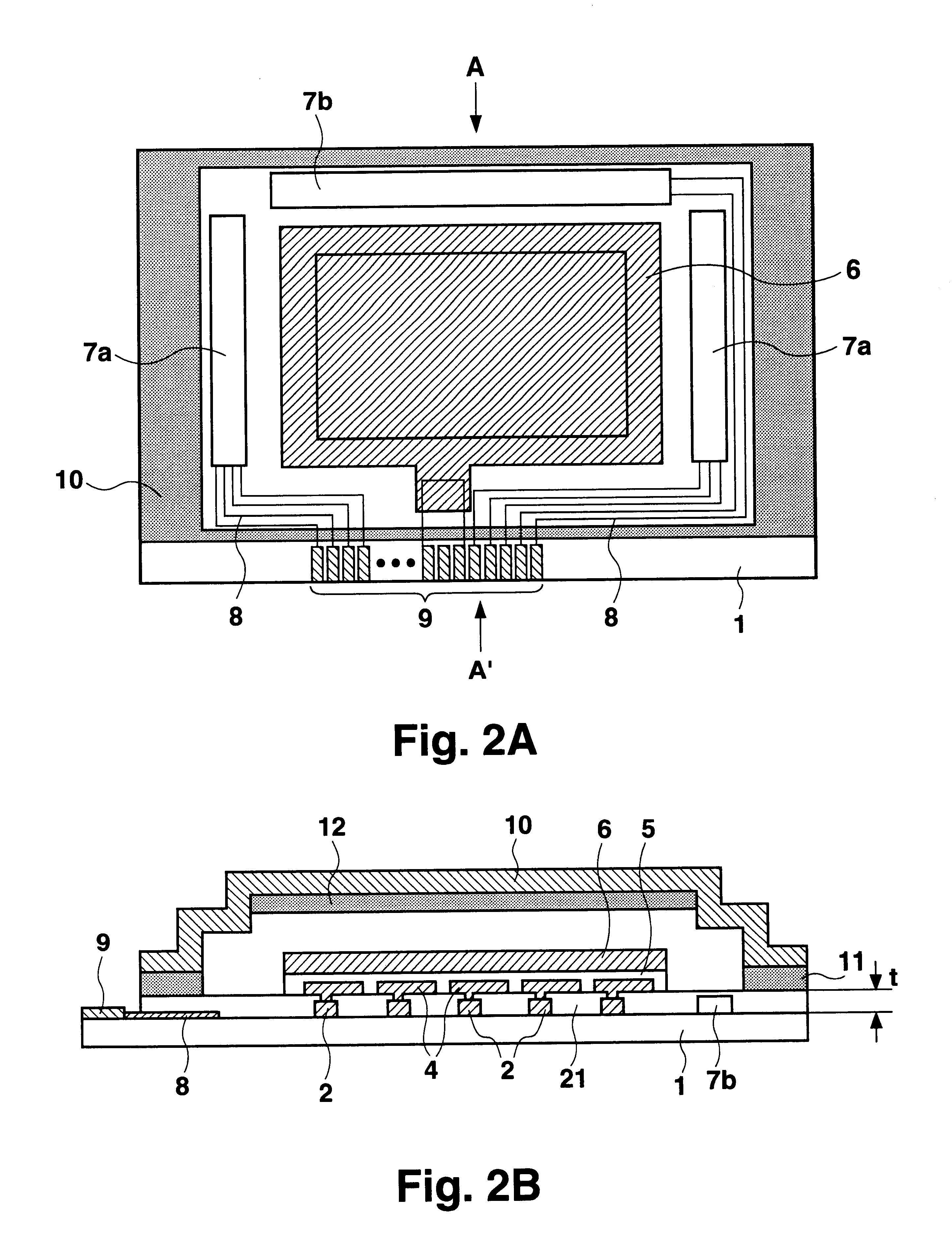
FIG. 2A is a plan view of an organic EL display device according to a preferred embodiment of the present invention, and FIG. 2B shows a cross-sectional view taken along line A-A' of FIG. 2A. Structures similar to those in the conventional device described earlier are labeled with the same reference numerals, and detailed explanation of those structures will not be repeated. Arranged on a transparent substrate for respective pixels are selective drive circuits 2 and pixel electrodes 4. An emissive layer 5 and a counter electrode 6 are disposed covering those structures. Surrounding the pixel region including the selective drive circuits 2, pixel electrodes 4, emissive layer 5, and counter electrode 6, driver circuits 7a,7b are arranged for controlling the selective drive circuits 2 and applying predetermined voltages to the pixel electrodes 4. The driver circuits 7 are connected to terminals 9 by wiring 8. A protective casing 10 is arranged covering the display region. In the presen...


PUM


Abstract

In a display device formed by adhering substrates facing one another using a seal, a buffer layer is disposed between the seal and a substrate to prevent separation between the substrates. Specifically, for example, a display region is configured by covering switching elements with a planarizing insulating film for planarization, then forming, in order, pixel electrodes, an emissive layer, and a counter electrode. The planarizing insulating film is extended beyond the display region to an area under the seal. The planarizing insulating film functions as the buffer layer to absorb the stress generated during curing of the seal, thereby preventing separation between the substrate and the protective casing.

Description

1. Field of the InventionThe present invention relates to a display device comprising a light-emitting layer such as an electroluminescence (hereinafter referred to as "EL") element disposed on a substrate, and particularly to a sealing structure for an organic EL display device.2. Description of the Prior ArtIn the recent years, organic EL display devices have gained attention as devices that may replace CRTs and LCDs. FIG. 1A is a plan view of a conventional organic EL display device, and FIG. 1B shows a cross-sectional view taken along line A-A' of FIG. 1A. A plurality of selective drive circuits 2 are disposed for respective pixels on a transparent substrate 1. A planarizing insulating film 3 is formed covering the selective drive circuits 2. A contact hole is created in the planarizing insulating film 3 in a position corresponding to each selective drive circuit 2. Each selective drive circuit 2 is connected to a pixel electrode 4 through this contact hole. An emissive layer 5 ...

Claims


Application Information

Patent Timeline
IPC IPC(8): H01L27/28H01L27/32H01L51/52H01L51/50G09F9/00H05B33/00H05B33/04H05B33/12
CPCH01L27/3244H01L51/5246H01L51/5243H01L51/5259Y10S428/917H10K59/12H10K50/8423H10K50/846H10K50/8426H05B33/04
Inventor NISHIKAWA, RYUJIYAMADA, TSUTOMU
Owner SANYO ELECTRIC CO LTD
Why Eureka
Try Eureka