Mold and method for producing the same

a mold and mold technology, applied in the field of mold and mold production method, can solve the problems of difficulty in releasing duplicated plates, mold chipping, and lowering the precision of pattern shape, so as to reduce the concentration of stress, improve the releasability of duplicated plates, and reduce the concentration of duplicated plates

Inactive Publication Date: 2010-08-26
FUJIFILM CORP
View PDF10 Cites 11 Cited by
  • Summary
  • Abstract
  • Description
  • Claims
  • Application Information

AI Technical Summary

Benefits of technology

[0038]According to the method for producing a mold of the invention, the presence of the release layer, which is made of the metal film containing a metal having an ionization tendency lower than that of hydrogen (for example, at least one metal selected from Pt, Os, Ir, Au, Ru and Pd), improves releasability of the duplicated plate with respect to the Si original plate. In other words, due to the presence of the release layer, which has an ionization tendency lower than that of hydrogen and thus is not easy to oxidize, a binding force between the Si original plate and the duplicated plate is reduced. This mitigates the concentration of stress at the ridge portions filling the groove portions of the groove-ridge pattern when the duplicated plate is released, thereby preventing generation of chipped ridge portions. Thus, a mold with good shape stability can be provided even when the groove-ridge pattern of the mold has a high aspect ratio.
[0039]Further, since the release layer is released as the duplicated plate from the Si original plate together with the metal substrate, the magnetic layer and / or the conductive layer formed after the release layer, repeated use of the Si original plate, which serves as an original mold of the groove-ridge pattern, can be achieved.
[0040]Furthermore, since the release layer is made of the metal having an ionization tendency lower than that of hydrogen, when the release layer is immersed in an acidic electroforming solution and a current is applied thereto during electroforming of the metal substrate, it does not dissolve in the electroforming solution. Thus, good releasability and conductivity are maintained, thereby allowing successful electroforming and releasing in the subsequent steps.
[0041]According to the mold of the invention, the surface of the groove-ridge pattern of the mold formed by the released duplicated plate is coated with the release layer, and therefore, adhesion defect, which occurs when an organic release agent is used, can be prevented.
[0042]Further, according to the invention, a fine groove-ridge pattern can be formed with high precision on a mold, thereby providing a mold with excellent transfer characteristics for magnetic transfer or shape transfer. In addition, use of the mold according to the invention allows transfer with stable quality.
[0043]That is, according to the invention, a mold with high reproducibility of a groove-ridge shape can be provided, which is free of deformation of ridge portions of the groove-ridge pattern even when the groove-ridge pattern has narrower and / or higher ridge portions. For example, as a mold for magnetic transfer, a master carrier which provides high quality signal through magnetic transfer can be provided. As a mold for shape transfer, a mold for nanoimprint, discrete track media or bit pattern media with high reproducibility of the transferred shape, or a stamper for high-quality optical disks, can be provided.

Problems solved by technology

Therefore, a large joining force is present between the Si original plate and the magnetic layer, and it is difficult to release the duplicated plate.
In this case, although the Ni conductive layer is easier to be released than the above-described magnetic layer, there still remains a problem that duplicated ridge portions of the groove-ridge pattern on the mold may be chipped and precision of the pattern shape may be lowered when increasingly finer groove-ridge patterns are formed on Si original plates.
Moreover, in the case where the substrate of the mold is formed through electroforming, the electroforming solution is acidic.
Therefore, when the Si original plate with the conductive layer formed thereon is immersed in the electroforming solution and a current is applied thereto, the conductive layer is dissolved by the acid of the electroforming solution and this causes poor electric conduction, which hinders formation of a desired substrate.
The above-described problems occur not only with master carriers for magnetic transfer, and are common among mold structures having a fine groove-ridge pattern on the surface.
In particular, a large adhesion force to the Si original plate is present at opposite side surfaces of the tip of each ridge portions, and this causes the concentration of the stress when the mold is released from the Si original plate, which may result in chipped ridge portions.
In addition, in the case of production of the mold for magnetic transfer, if the magnetic layer is formed in the groove portions of the groove-ridge pattern of the Si original plate, as described above, a strong adhesion force is generated between the magnetic layer, such as a FeCo layer, or the like, and the Si original plate, and this also causes the concentration of the stress which may result in chipped ridge portions.
However, although the release agent provides improved releasability, the release agent may remain on the surfaces of the Si original plate and the mold and may cause an adhesion defect during a magnetic transfer step, etc.

Method used


Image

  • Mold and method for producing the same
  • Mold and method for producing the same
  • Mold and method for producing the same

Examples


second embodiment

of Method for Producing Master Carrier

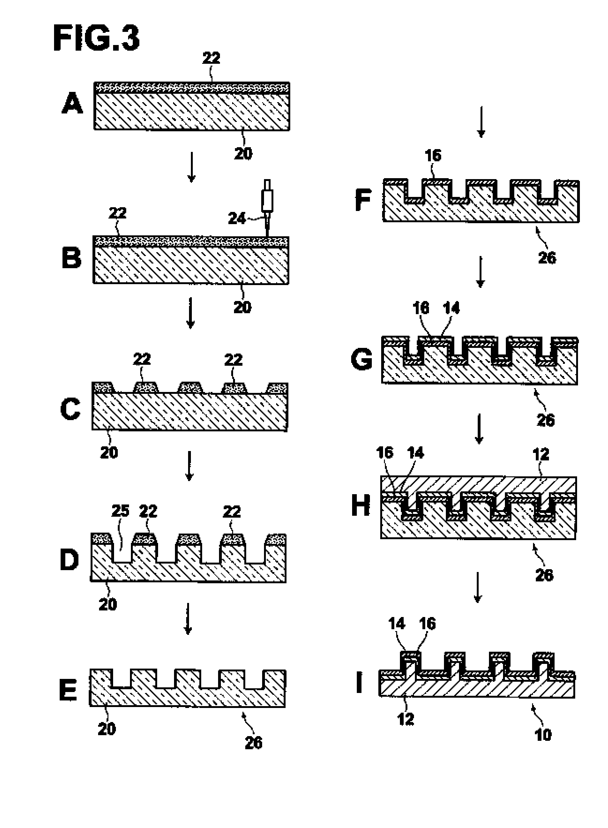
[0091]Next, a method for producing a master carrier according to another embodiment is described based on FIG. 5. This production method differs from the method described above with reference to

[0092]FIG. 3 in that, after the release layer has been formed and before the master substrate (metal substrate) is formed, a filling layer is formed to fill the groove portions of the groove-ridge pattern of the Si original plate. That is, this method includes the same steps as the steps shown at “A” to “G” in FIG. 3 of the above-described method. It should be noted that the same components as those in the above-described embodiment are denoted by the same reference numerals, and explanations thereof are omitted unless otherwise required.

[0093]FIG. 5 shows at “A” a schematic sectional view of the Si original plate in a state where the release layer 16 and the magnetic layer 14 are formed in this order after the groove-ridge pattern has been formed on the ...

example 1

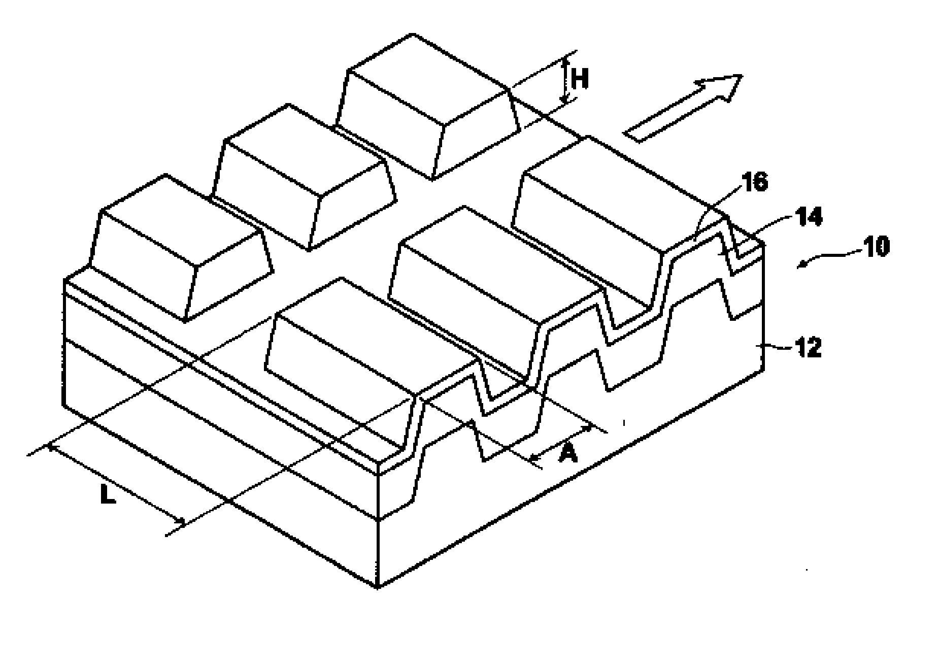
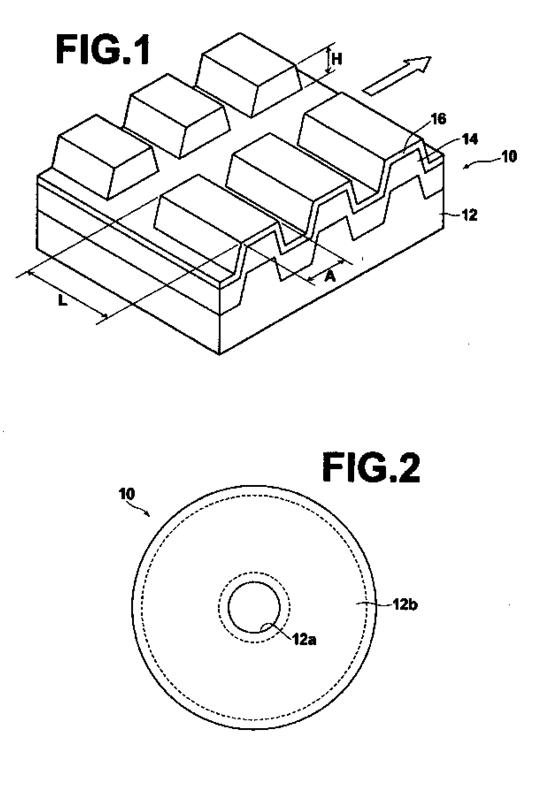
[0104]As an example of the layer structure of a mold (master carrier) for magnetic transfer, a 3 nm-thick Pt release layer and a 20 nm-thick FeCo magnetic layer were formed in this order through sputtering on the surface of a Si original plate, which had on the surface thereof a fine groove pattern having a half width of 30 nm and a height of 100 nm. Then, a 150 μm-thick Ni master substrate was formed through electroforming on the Si original plate having the two layers, the Pt release layer (3 nm) and the FeCo layer (20 nm), formed thereon to form a duplicated plate. The duplicated plate was released from the Si original plate to provide a master carrier for magnetic transfer having on the surface thereof a ridge pattern, which is a reverse pattern of the groove pattern, and including the magnetic layer and the Pt release layer formed on the surface of the reverse pattern.

example 2

[0105]As an example of the layer structure of a mold for discrete track media, a 9 nm-thick Ru release layer was formed through sputtering on the surface of the Si original plate, which had on the surface thereof a fine groove pattern having a half width of 20 nm and a height of 60 nm. Then, a 150 μm-thick Ni substrate was formed through electroforming on the Si original plate with the 9 nm-thick Ru release layer formed thereon to form a duplicated plate. The duplicated plate was released from the Si original plate to provide a mold for shape transfer having on the surface thereof a ridge pattern, which is a reverse pattern of the groove pattern, and including the Ru release layer formed on the surface of the reverse pattern.


PUM

PropertyMeasurementUnit
thicknessaaaaaaaaaa
thicknessaaaaaaaaaa
thicknessaaaaaaaaaa

Abstract

A method for producing a mold having a fine groove-ridge pattern on the surface thereof is disclosed. The method includes: a release layer forming step of forming, on a surface of a Si original plate having a groove-ridge pattern, a release layer made of a metal film containing a metal having an ionization tendency lower than that of hydrogen (for example, at least one metal selected from the group consisting of Pt, Os, Ir, Au, Ru and Pd); an electroforming step of electroforming, after the release layer has been formed, a metal substrate forming a mold; and a releasing step of releasing a duplicated plate including the release layer and the metal substrate from the Si original plate after the electroforming step.

Description

BACKGROUND OF THE INVENTION[0001]1. Field of the Invention[0002]The present invention relates to a mold and a method for producing the mold. More particularly, the present invention relates to a method for producing a mold having a fine groove-ridge pattern on the surface thereof and a mold produced by the method, such as a magnetic transfer mold (master carrier) used during a step of magnetically transferring a magnetic information pattern (format information, etc.) to a medium to which information is transferred (also referred to as a slave medium), which is one of the steps of a process for producing a magnetic recording medium, such as a magnetic disk used in a hard disk device, a mold used to produce discrete track media (DTM), or a mold used for nanoimprint.[0003]2. Description of the Related Art[0004]A magnetic disk used in a hard disk drive is typically produced by writing, on a slave medium, format information and address information before it is disposed in the drive. The ...

Claims


Application Information

Patent Timeline
Patent Type & Authority Applications(United States)
IPC IPC(8): B29C59/02C25D5/16C23C14/46
CPCB82Y10/00C25D1/10G11B7/261G11B5/743G11B5/865C25D1/20
Inventor KIDO, TAKEO
Owner FUJIFILM CORP
Why Eureka
Try Eureka